- 您现在的位置:买卖IC网 > PDF目录189002 > NAND08GR4B2BZC6T (STMICROELECTRONICS) 512M X 16 FLASH 1.8V PROM, 35 ns, PBGA63 PDF资料下载
参数资料
| 型号: | NAND08GR4B2BZC6T |
| 厂商: | STMICROELECTRONICS |
| 元件分类: | PROM |
| 英文描述: | 512M X 16 FLASH 1.8V PROM, 35 ns, PBGA63 |
| 封装: | 9.50 X 12 MM, 1.40 MM HEIGHT, 0.80 MM PITCH, ROHS COMPLIANT, LFBGA-63 |
| 文件页数: | 17/59页 |
| 文件大小: | 998K |
| 代理商: | NAND08GR4B2BZC6T |
第1页第2页第3页第4页第5页第6页第7页第8页第9页第10页第11页第12页第13页第14页第15页第16页当前第17页第18页第19页第20页第21页第22页第23页第24页第25页第26页第27页第28页第29页第30页第31页第32页第33页第34页第35页第36页第37页第38页第39页第40页第41页第42页第43页第44页第45页第46页第47页第48页第49页第50页第51页第52页第53页第54页第55页第56页第57页第58页第59页
NAND512-B, NAND01G-B, NAND02G-B, NAND04G-B, NAND08G-B
24/59
Copy Back Program
The Copy Back Program operation is used to copy
the data stored in one page and reprogram it in an-
other page.
The Copy Back Program operation does not re-
quire external memory and so the operation is
faster and more efficient because the reading and
loading cycles are not required. The operation is
particularly useful when a portion of a block is up-
dated and the rest of the block needs to be copied
to the newly assigned block.
If the Copy Back Program operation fails an error
is signalled in the Status Register. However as the
standard external ECC cannot be used with the
Copy Back Program operation bit error due to
charge loss cannot be detected. For this reason it
is recommended to limit the number of Copy Back
Program operations on the same data and or to
improve the performance of the ECC.
The Copy Back Program operation requires four
steps:
1.
The first step reads the source page. The
operation copies all 1056 Words/ 2112 Bytes
from the page into the Data Buffer. It requires:
–
one bus write cycle to setup the command
–
4 bus write cycles to input the source page
address
–
one bus write cycle to issue the confirm
command code
2.
When the device returns to the ready state
(Ready/Busy High), the next bus write cycle of
the command is given with the 4 bus cycles to
input the target page address. Refer to Table
11. for the addresses that must be the same
for the Source and Target pages.
3.
Then the confirm command is issued to start
the P/E/R Controller.
The Data Input cycle for modifying the source
page is performed as shown in Figure 14. After a
Copy Back Program operation, a partial-page pro-
gram is not allowed in the target page until the
block has been erased.
See Figure 14. for an example of the Copy Back
Program operation.
A data input cycle to modify a portion or a multiple
distant portion of the source page, is shown in Fig-
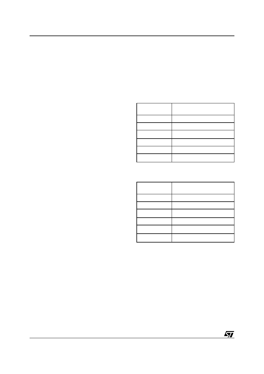
Table 11. Copy Back Program x8 Addresses
Note: 1. DD = Dual Die, QD = Quadruple Die.
Table 12. Copy Back Program x16 Addresses
Note: 1. DD = Dual Die, QD = Quadruple Die.
Density
Same Address for Source and
Target Pages
512 Mbit
no constraint
1 Gbit
no constraint
2 Gbit DD(1)
A28
2 Gbit
no constraint
4 Gbit DD
A29
8 Gbit QD(1)
A29,A30
Density
Same Address for Source and
Target Pages
512 Mbit
no constraint
1 Gbit
no constraint
2 Gbit DD(1)
A27
2 Gbit
no constraint
4 Gbit DD(1)
A28
8 Gbit QD(1)
A28,A29
相关PDF资料 |
PDF描述 |
|---|---|
| NAND08GR4B3BN1 | 512M X 16 FLASH 1.8V PROM, 35 ns, PDSO48 |
| NAND512R3B3BZA6E | 64M X 8 FLASH 1.8V PROM, 35 ns, PBGA63 |
| NAND512W3B3BN6E | 64M X 8 FLASH 3V PROM, 35 ns, PDSO48 |
| NAND512W3B3BZA6E | 64M X 8 FLASH 3V PROM, 35 ns, PBGA63 |
| NAND512W3B3AN1 | 64M X 8 FLASH 3V PROM, 35 ns, PDSO48 |
相关代理商/技术参数 |
参数描述 |
|---|---|
| NAND08GW3B2AN6E | 功能描述:闪存 4 GBit 2112 Byte 1056 WP 1.8v/3v RoHS:否 制造商:ON Semiconductor 数据总线宽度:1 bit 存储类型:Flash 存储容量:2 MB 结构:256 K x 8 定时类型: 接口类型:SPI 访问时间: 电源电压-最大:3.6 V 电源电压-最小:2.3 V 最大工作电流:15 mA 工作温度:- 40 C to + 85 C 安装风格:SMD/SMT 封装 / 箱体: 封装:Reel |
| NAND08GW3B2AN6F | 功能描述:闪存 4 GB 2112B 1056 Word Pg 1.8V/3V RoHS:否 制造商:ON Semiconductor 数据总线宽度:1 bit 存储类型:Flash 存储容量:2 MB 结构:256 K x 8 定时类型: 接口类型:SPI 访问时间: 电源电压-最大:3.6 V 电源电压-最小:2.3 V 最大工作电流:15 mA 工作温度:- 40 C to + 85 C 安装风格:SMD/SMT 封装 / 箱体: 封装:Reel |
| NAND08GW3B2BN6E | 制造商:Micron Technology Inc 功能描述:NAND & S.MEDIA FLASH - Trays |
| NAND08GW3B2CN6E | 功能描述:闪存 NAND & S.MEDIA FLASH RoHS:否 制造商:ON Semiconductor 数据总线宽度:1 bit 存储类型:Flash 存储容量:2 MB 结构:256 K x 8 定时类型: 接口类型:SPI 访问时间: 电源电压-最大:3.6 V 电源电压-最小:2.3 V 最大工作电流:15 mA 工作温度:- 40 C to + 85 C 安装风格:SMD/SMT 封装 / 箱体: 封装:Reel |
| NAND08GW3B2CN6F | 功能描述:闪存 NAND & S.MEDIA FLASH RoHS:否 制造商:ON Semiconductor 数据总线宽度:1 bit 存储类型:Flash 存储容量:2 MB 结构:256 K x 8 定时类型: 接口类型:SPI 访问时间: 电源电压-最大:3.6 V 电源电压-最小:2.3 V 最大工作电流:15 mA 工作温度:- 40 C to + 85 C 安装风格:SMD/SMT 封装 / 箱体: 封装:Reel |
发布紧急采购,3分钟左右您将得到回复。