参数资料
| 型号: | NB4L339MNGEVB |
| 厂商: | ON Semiconductor |
| 文件页数: | 2/7页 |
| 文件大小: | 0K |
| 描述: | BOARD EVAL FOR NB4L339MNG |
| 标准包装: | 1 |
| 系列: | * |
�� �
�
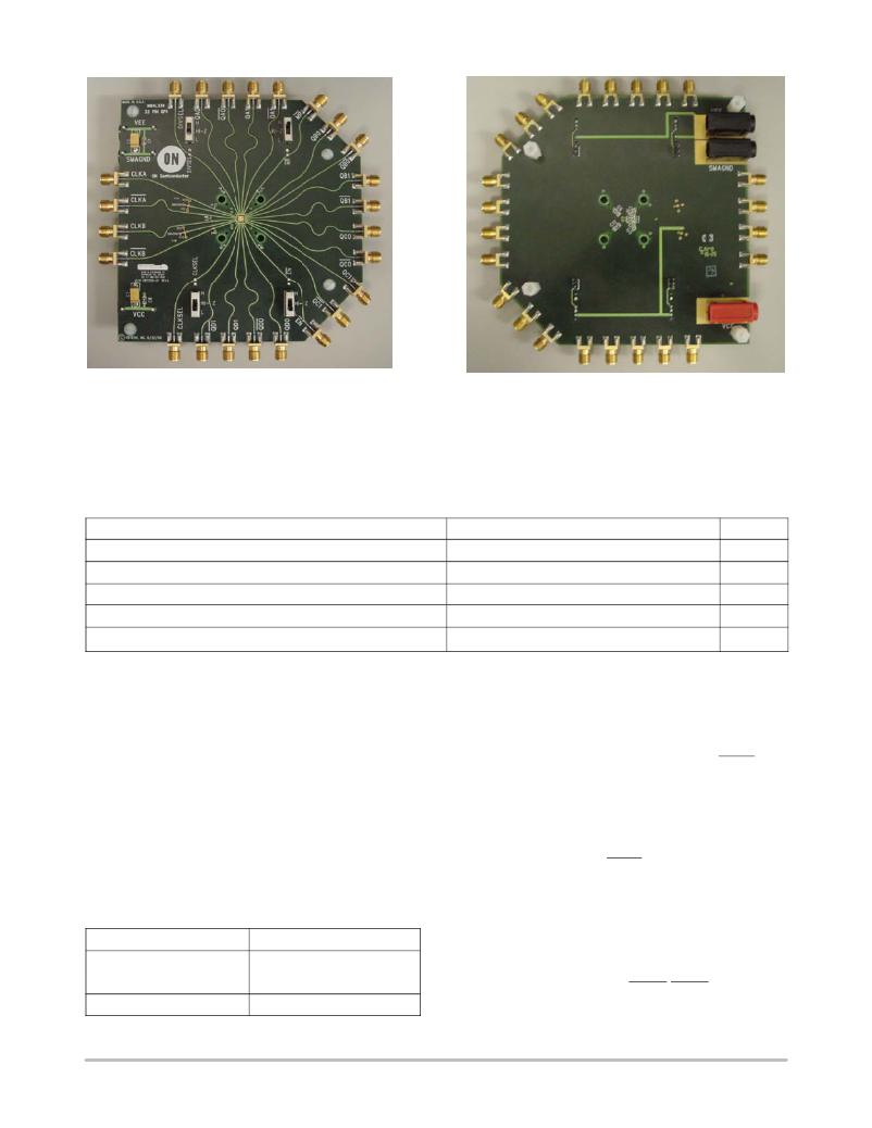
�NB4L339MNGEVB�
�Top� View�
�Figure� 1.� NB4L339MNGEVB� Evaluation� Board�
�Lab� Setup� for� Time� Domain� Measurements�
�Table� 1.� Basic� Lab� Equipment�
�Bottom� View�
�Description�
�Power� Supply� with� 4� outputs�
�Oscilloscope� and/or� Frequency� counter�
�Differential� Signal� Generator�
�Matched� High� Speed� Cables� with� SMA� Connectors�
�Digital� Voltmeter,� Power� supply� cables�
�Example� Equipment�
�HP6624A�
�TDS8000� with� 80E01� Sampling� Head�
�Agilent� 8133A,� Advantest� D3186�
�Storm,� Semflex�
�Qty�
�1�
�1�
�1�
�6� Pair�
�Lab� Setup�
�A� typical� lab� setup� for� taking� time� domain� measurements�
�in� differential� mode� operation� is� shown� in� Figure� 2.� The�
�following� steps� should� be� followed� for� proper� equipment�
�setup:�
�Step� 1:� Connect� Power�
�Three� power� levels� must� be� provided� to� the� board,� V� CC� ,�
�V� EE� ,� and� SMAGND� via� the� banana� jack� connectors� on� the�
�bottom� of� the� board.� Bypass� capacitors� are� installed� from�
�V� CC� to� SMAGND� and� V� EE� to� SMAGND� at� the� banana� jacks�
�and� the� deivce� pins.� Using� the� split� power� supply� mode,�
�GND� =� V� TT� =� V� CC� ?� 2.0� V.� The� exposed� pad� of� the� QFN� ?� 32�
�package� is� connected� to� V� EE� .�
�Table� 2.� NB4L339� Power� Supply� Connections�
�1.� SMAGND� (V� TT� )� is� the� termination� supply� for� the� LVPECL� outputs�
�only,� not� to� be� confused� with� the� device� ground� pin� (V� EE� ).�
�Step� 2:� Connect� Inputs�
�For� Differential� Mode:�
�Connect� the� differential� output� of� the� signal� generator� to�
�the� differential� input� of� the� device� (CLKx� and� CLKx).� The�
�differential� clock� inputs� of� the� NB4L339� incorporate�
�internal� 50� W� termination� resistors.�
�For� Single� ?� Ended� Mode:�
�Connect� the� single� ?� ended� output� of� the� generator� to� the�
�CLKx� input� of� the� device.� Vth� must� be� applied� to� the�
�complementary� input� (CLKx)� when� operating� in�
�single� ?� ended� mode.� Refer� to� the� device� datasheet� for� details�
�on� single� ?� ended� operation.�
�The� VTA� and� VTB� termination� pins� each� have� a� trace�
�3.3� V� Setup�
�V� CC� =� 2.0� V�
�V� TT� =� SMAGND� =� 0� V�
�V� EE� =� ?� 1.3� V�
�2.5� V� Setup�
�V� CC� =� 2.0� V�
�V� TT� =� SMAGND� =� 0� V�
�V� EE� =� ?� 0.5� V�
�from� package� pin� to� a� node� where� it� can� be� connected� to�
�either� VCC,� VEE� or� SMAGND,� depending� on� the� user� ’s�
�need.�
�NOTE:� Inputs� CLKA/B� and� CLKA/CLKB� must� be�
�signal� driven� or� auto� oscillation� may� result.�
�http://onsemi.com�
�2�
�相关PDF资料 |
PDF描述 |
|---|---|
| NB4N11MDTEVB | BOARD EVAL FOR NB4N11MD |
| NB4N441MNGEVB | BOARD EVAL NB4N441MNG |
| NB4N507ADEVB | BOARD EVAL FOR BBG NB4N507AD |
| NB4N855SMEVB | CUSTOMER EVALUATION BRD |
| NB6L11MMNGEVB | BOARD EVAL NB6L11MMN CLK BUFFER |
相关代理商/技术参数 |
参数描述 |
|---|---|
| NB4L339MNR2G | 制造商:ONSEMI 制造商全称:ON Semiconductor 功能描述:2.5 V / 3.3 V Differential 2:1 Clock IN to Differential LVPECL Clock Generator / Divider / Fan−Out Buffer |
| NB4L339MNR4G | 功能描述:时钟驱动器及分配 2.7V 622MHZ CLK DIST RoHS:否 制造商:Micrel 乘法/除法因子:1:4 输出类型:Differential 最大输出频率:4.2 GHz 电源电压-最大: 电源电压-最小:5 V 最大工作温度:+ 85 C 封装 / 箱体:SOIC-8 封装:Reel |
| NB4L52 | 制造商:ONSEMI 制造商全称:ON Semiconductor 功能描述:2.5 V/3.3 V/5.0 V Differential Data/Clock D Flip-Flop with Reset Multi-Level Inputs to LVPECL Translator w/ Internal Termination |
| NB4L52_07 | 制造商:ONSEMI 制造商全称:ON Semiconductor 功能描述:2.5 V/3.3 V/5.0 V Differential Data/Clock D Flip-Flop with Reset Multi-Level Inputs to LVPECL Translator w/ Internal Termination |
| NB4L52MNG | 功能描述:转换 - 电压电平 ANA ECL D FF W/DIFF RESET RoHS:否 制造商:Micrel 类型:CML/LVDS/LVPECL to LVCMOS/LVTTL 传播延迟时间:1.9 ns 电源电流:14 mA 电源电压-最大:3.6 V 电源电压-最小:3 V 最大工作温度:+ 85 C 安装风格:SMD/SMT 封装 / 箱体:MLF-8 |
发布紧急采购,3分钟左右您将得到回复。