参数资料
| 型号: | NB4N441MNGEVB |
| 厂商: | ON Semiconductor |
| 文件页数: | 17/18页 |
| 文件大小: | 0K |
| 描述: | BOARD EVAL NB4N441MNG |
| 标准包装: | 1 |
| 系列: | * |
�� �
�
�NB4N441MNGEVB�
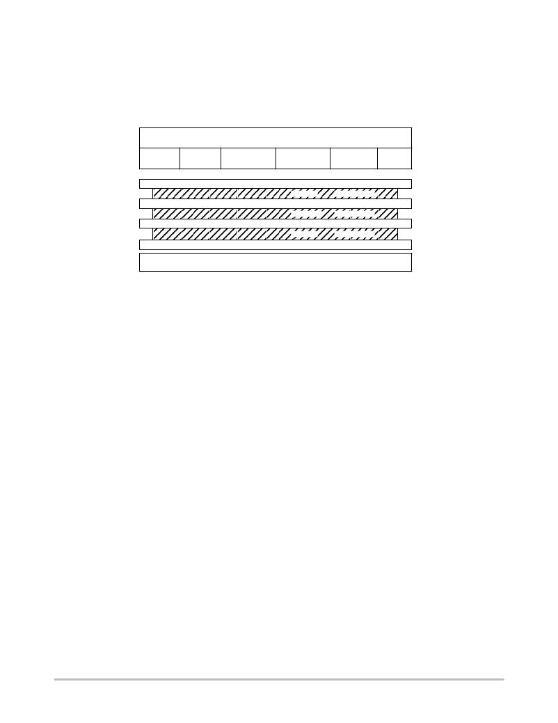
�LAMINATION� STACK�
�L1�
�L2�
�L3�
�L4�
�Signal�
�SMAGND�
�V� CC� and� DUTGND�
�DUTGND� and� Signal�
�LAMINATION� DIAGRAM�
�Layer�
�Number�
�1�
�Layer�
�Name�
�TOP�
�Copper�
�Thickness�
�1/2� OZ.�
�Dielectric�
�Thickness�
�Layer�
�Material�
�Trace�
�Width�
�0.012�
�0.006�
�GETEK�
�2�
�3�
�4�
�SMAGND�
�PWR�
�DUTGND�
�1� OZ.�
�1� OZ.�
�1/2� OZ.�
�Adjust�
�0.006�
�GETEK�
�GETEK�
�???�
�???�
�0.011�
�FINISHED� PCB� THICKNESS� TO� BE:�
�0.64� ±� 0.003�
�ASSEMBLY� NOTES:�
�Notes� (Unless� Otherwise� Specified)�
�Material:�
�1.� GETEK� Laminate� Epoxy/Polyphenylene� Oxide�
�Resin� Type� NEMA� FR� ?� 4� (IPC� ?� L� ?� 1088/04).� See�
�Layer� Table.� Inner� Layers:� 1� oz.� Copper� clad�
�Outer� Layers:� 1/2� oz.� Copper� Foil� Plated� to� 1�
�1/2� oz� finished.�
�2.� Refer� to� Stacking� Diagram� for� Finished� Board�
�Thickness.�
�Tooling:�
�3.� Photo� etch� circuitry� per� artwork� drill� locations�
�controlled� by� drill� file.drl� fabrication� print.�
�4.� The� dielectric� thickness� of� the� controlled�
�impedance� layers� is� for� reference� only.� Final�
�acceptance� shall� be� determined� by� these� layer� pairs�
�having� a� characteristic� impedance� of� 52.5� W�
�$� 10%.� The� vendor� can� make� width� adjustments�
�on� only� the� critical� conductor� widths� of� $� 0.0005.�
�All� other� adjustments� must� have� prior� approval�
�from� Baldwin� Tech� Layer� Grouping� (1.2).�
�5.� Finished� conductor� width� to� be� 0.012”.�
�Finish:�
�6.� Plating� Specification:� Electrodeposited� hard� gold�
�plate,� Type� 1� (99.7%� min� gold)� Grade� C� (Knoop�
�Hardness� 130� ?� 200),� Class� 1� (50� ?� 100� micro� ?� inches�
�thick)� in� accordance� with� MIL� ?� G� ?� 4520C� and�
�ANSI/IPC� ?� A� ?� 6000.� Section� 4.0� (surface� placing�
�acceptability� requirements),� Class� 3� (50� ?� 100�
�micro� ?� inches� thick)� over� electrodeposited� nickel�
�plate� in� accordance� with� ANSI/IPC� ?� A� ?� 6000,�
�Section� 4.0,� Class� 3� (200� ?� 600� micro� ?� inches� thick).�
�7.� Drill� sizes� are� finished.� Plated� through� holes� to�
�have� a� minimum� barrel� plating� of� 0.0008� in.�
�8.� Board� twist� and� warp� not� to� exceed� 0.005� in� (5%)�
�per� linear� inch.� Front� to� back� registration� to� be�
�within� 0.003� in.�
�9.� True� position� tolerance� shall� be� determined� by� a�
�minimum� anular� ring� of� 0.005� in.�
�10.� Plated� holes� shall� not� be� rough� or� irregular� so� as� to�
�hinder� proper� solder� wicking.�
�11.� Soldermask:� Green� LPI:� B0�
�12.� Apply� Legend� (SILKSCREEN)� to� both� sides� using�
�a� nonconductive,� white,� Epoxy� based� ink� per�
�artwork.�
�13.� No� board� shop� logo� on� board.�
�14.� Each� PCB� shall� be� serialized,� in� legend,� in� the� area�
�shown,� as� follow:� 0005� ?� 1� ?� 1� (Sequential� Number�
�(assigned� per� panel)� ?� Panel� Number� (assigned� per�
�log)� ?� Year� and� Week).�
�Testing:�
�15.� Final� Electrical� Test� shall� be� preformed� per�
�provided� IPC� ?� 356� netlist.� The� PCB� shall� have� a�
�verification� stamp.� Connectivity� to� be� verified�
�against� IPC� format� net� list.�
�16.� A� TDR� report� for� each� layer� shall� be� provided� by�
�vendor� at� time� of� shipment.�
�http://onsemi.com�
�17�
�相关PDF资料 |
PDF描述 |
|---|---|
| NB4N507ADEVB | BOARD EVAL FOR BBG NB4N507AD |
| NB4N855SMEVB | CUSTOMER EVALUATION BRD |
| NB6L11MMNGEVB | BOARD EVAL NB6L11MMN CLK BUFFER |
| NB6L239MNEVB | BOARD EVAL BBG NB6L239MND |
| NB7L32MMNEVB | BOARD EVAL FOR NB7L32MM |
相关代理商/技术参数 |
参数描述 |
|---|---|
| NB4N441MNR2G | 功能描述:锁相环 - PLL MLTPRTCL PLL CLK SYN RoHS:否 制造商:Silicon Labs 类型:PLL Clock Multiplier 电路数量:1 最大输入频率:710 MHz 最小输入频率:0.002 MHz 输出频率范围:0.002 MHz to 808 MHz 电源电压-最大:3.63 V 电源电压-最小:1.71 V 最大工作温度:+ 85 C 最小工作温度:- 40 C 封装 / 箱体:QFN-36 封装:Tray |
| NB4N507A | 制造商:未知厂家 制造商全称:未知厂家 功能描述:3.3V/5V, 50 MHz to 200 MHz PECL Clock Synthesizer |
| NB4N507A_06 | 制造商:ONSEMI 制造商全称:ON Semiconductor 功能描述:3.3V/5V, 50 MHz to 200 MHz PECL Clock Synthesizer |
| NB4N507AD | 功能描述:锁相环 - PLL 3.3V/5V PECL Clock RoHS:否 制造商:Silicon Labs 类型:PLL Clock Multiplier 电路数量:1 最大输入频率:710 MHz 最小输入频率:0.002 MHz 输出频率范围:0.002 MHz to 808 MHz 电源电压-最大:3.63 V 电源电压-最小:1.71 V 最大工作温度:+ 85 C 最小工作温度:- 40 C 封装 / 箱体:QFN-36 封装:Tray |
| NB4N507ADEVB | 功能描述:BOARD EVAL FOR BBG NB4N507AD RoHS:是 类别:编程器,开发系统 >> 评估演示板和套件 系列:* 标准包装:1 系列:PCI Express® (PCIe) 主要目的:接口,收发器,PCI Express 嵌入式:- 已用 IC / 零件:DS80PCI800 主要属性:- 次要属性:- 已供物品:板 |
发布紧急采购,3分钟左右您将得到回复。