- 您现在的位置:买卖IC网 > PDF目录22206 > NCP1653DR2 (ON Semiconductor)IC CTRLR PFC CURRENT MODE 8SOIC PDF资料下载
参数资料
| 型号: | NCP1653DR2 |
| 厂商: | ON Semiconductor |
| 文件页数: | 12/19页 |
| 文件大小: | 0K |
| 描述: | IC CTRLR PFC CURRENT MODE 8SOIC |
| 产品变化通告: | LTB Notification 03/Jan/2008 |
| 标准包装: | 1 |
| 模式: | 连续导电(CCM) |
| 频率 - 开关: | 90kHz ~ 110kHz |
| 电源电压: | 8.75 V ~ 18 V |
| 工作温度: | -40°C ~ 125°C |
| 安装类型: | 表面贴装 |
| 封装/外壳: | 8-SOIC(0.154",3.90mm 宽) |
| 供应商设备封装: | 8-SOICN |
| 包装: | 剪切带 (CT) |
| 其它名称: | NCP1653DR2OSCT |
�� �
�
�NCP1653,� NCP1653A�
�As� a� result,� the� on� time� t� 1� is� reduced.� Reduction� of� on� time�
�makes� the� loss� of� the� inductor� and� power� MOSFET� smaller.�
�Hence,� it� allows� cheaper� cost� in� the� inductor� and� power�
�depending� on� different� values� of� V� ac� and� P� out� .� The� follower�
�boost� operating� area� is� illustrated� in� Figure� 33.�
�MOSFET� or� allows� the� circuit� components� to� operate� at� a�
�lower� stress� condition� in� most� of� the� time.�
�Vout�
�96%� I� ref� R� FB�
�Pout(min)�
�Pout(max)�
�Output� Feedback�
�The� output� voltage� V� out� of� the� PFC� circuit� is� sensed� as� a�
�feedback� current� I� FB� flowing� into� the� FB� pin� (Pin� 1)� of� the�
�device.� Since� the� FB� pin� voltage� V� FB1� is� much� smaller� than�
�V� out� ,� it� is� usually� neglected.�
�V� in�
�1�
�V� ac(min)�
�2�
�1.� P� out� increases,� V� out� decreases�
�2.� V� ac� decreases,� V� out� decreases�
�V� ac(max)� V� ac�
�IFB� +� out�
�[� out�
�V� *� VFB1�
�RFB�
�V�
�RFB�
�(eq.14)�
�Figure� 33.� Follower� Boost� Region�
�Icontrol(max)� Vout�
�Icontrol� +�
�1� *�
�0.04�
�Vout� +�
�RM� RCS� (eq.17)�
�)� R�
�2� RS� R� vac� Vref� Icontrol(max)�
�FB� Iref�
�where� R� FB� is� the� feedback� resistor� across� the� FB� pin�
�(Pin� 1)� and� the� output� voltage� referring� to� Figure� 2.�
�Then,� the� feedback� current� I� FB� represents� the� output�
�voltage� V� out� and� will� be� used� in� the� output� voltage�
�regulation,� undervoltage� protection� (UVP),� and�
�overvoltage� protection� (OVP).�
�Output� Voltage� Regulation�
�Feedback� current� I� FB� which� represents� the� output� voltage�
�V� out� is� processed� in� a� function� with� a� reference� current�
�(I� ref� =� 200� m� A� typical)� as� shown� in� regulation� block�
�function� in� Figure� 32.� The� output� of� the� voltage� regulation�
�block,� low� ?� pass� filter� on� V� control� pin� and� the� I� control� =�
�V� control� /� R� 1� block� is� in� Figure� 30� is� control� current� I� control� .�
�And� the� input� is� feedback� current� I� FB� .� It� means� that� I� control�
�is� the� output� of� I� FB� and� it� can� be� described� as� in� Figure� 32.�
�There� are� three� linear� regions� including:� (1)� I� FB� <� 96%� �
�I� ref� ,� (2)� 96%� � I� ref� <I� FB� <� I� ref� ,� and� (3)� I� FB� >� I� ref� .� They� are�
�discussed� separately� as� follows:�
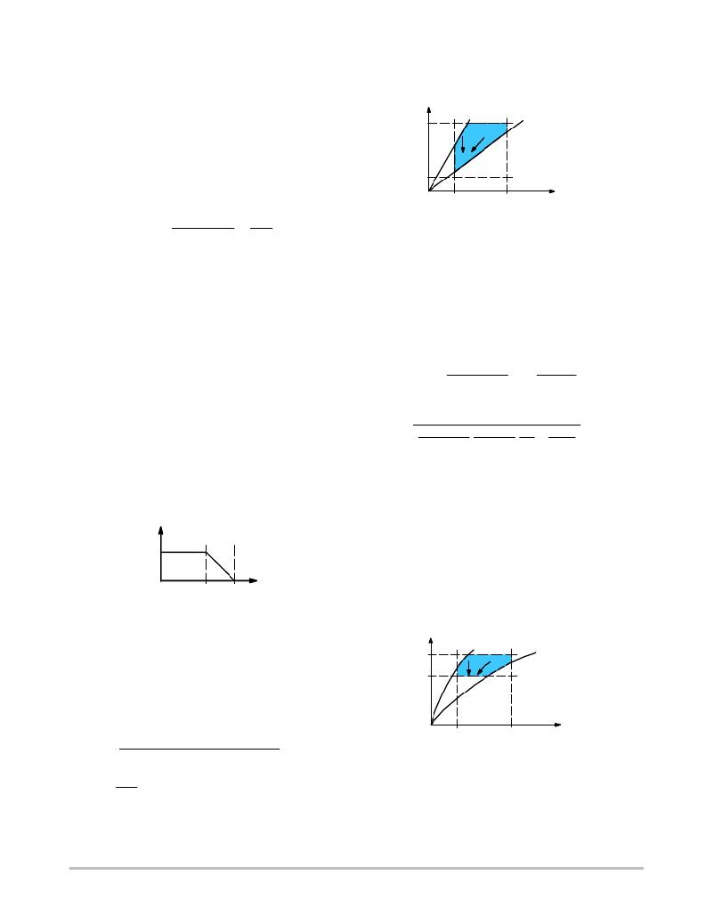
�Region� (2):� 96%� � I� ref� <� I� FB� <� I� ref�
�When� I� FB� is� between� 96%� and� 100%� of� I� ref� (i.e.,� 96%� R� FB�
�� I� ref� <� V� out� <� R� FB� � I� ref� ),� the� NCP1653� operates� in� constant�
�output� voltage� mode� which� is� similar� to� the� follower� boost�
�mode� characteristic� but� with� narrow� output� voltage� range.�
�The� regulation� block� output� V� reg� decreases� linearly� with�
�I� FB� in� the� range� from� 96%� of� I� ref� to� I� ref� .� It� gives� a� linear�
�function� of� I� control� in� (eq.16).�
�(eq.16)�
�RFB� Iref�
�Resolving� (eq.16)� and� (eq.13),�
�Vac�
�0.04� Pout� Vac�
�h�
�According� to� (eq.17),� output� voltage� V� out� becomes� R� FB�
�×� I� ref� when� power� is� low� (P� out� ≈� 0).� It� is� the� maximum� value�
�of� V� out� in� this� operating� region.� Hence,� it� can� be� concluded�
�that� output� voltage� increases� when� power� decreases.� It� is�
�I� control(max)�
�I� control�
�similar� to� the� follower� boost� characteristic� in� (eq.15).� On�
�the� other� hand� in� (eq.17),� output� voltage� V� out� becomes� R� FB�
�� I� ref� when� RMS� input� voltage� V� ac� is� very� high.� It� is� the�
�maximum� value� of� V� out� in� this� operating� region.� Hence,� it�
�can� also� be� concluded� that� output� voltage� increases� when�
�96%� I� ref�
�I� ref�
�I� FB�
�RMS� input� voltage� increases.� It� is� similar� to� another�
�follower� boost� characteristic� in� (eq.15).� This� characteristic�
�Vout� +� h�
�Vac�
�Pout�
�Pout(max)�
�Figure� 32.� Regulation� Block�
�Region� (1):� I� FB� <� 96%� � I� ref�
�When� I� FB� is� less� than� 96%� of� I� ref� (i.e.,� V� out� <� 96%� R� FB�
�� I� ref� ),� the� NCP1653� operates� in� follower� boost� mode.� The�
�regulation� block� output� V� reg� is� at� its� maximum� value.�
�I� control� becomes� its� maximum� value� (i.e.,� I� control� =�
�I� control(max)� =� I� ref� /2� =� 100� m� A)� which� is� a� constant.� (eq.13)�
�becomes� (eq.15).�
�2 RS R vac Icontrol(max) Vref Vac�
�RM� RCS� Pout�
�(eq.15)�
�T�
�The� output� voltage� V� out� is� regulated� at� a� particular� level�
�with� a� particular� value� of� RMS� input� voltage� V� ac� and� output�
�power� P� out� .� However,� this� output� level� is� not� constant� and�
�is� illustrated� in� Figure� 34.�
�Vout� Pout(min)�
�I� ref� R� FB�
�1� 2�
�96%� I� ref� R� FB�
�1.� P� out� increases,� V� out� decreases�
�2.� V� ac� decreases,� V� out� decreases�
�V� ac(min)� V� ac(max)� V� ac�
�Figure� 34.� Constant� Output� Voltage� Region�
�Region� (3):� I� FB� >� I� ref�
�When� I� FB� is� greater� than� I� ref� (i.e.,� V� out� >� R� FB� � I� ref� ),� the�
�NCP1653� provides� no� output� or� zero� duty� ratio.� The�
�regulation� block� output� V� reg� becomes� 0� V.� I� control� also�
�becomes� zero.� The� multiplier� voltage� V� M� in� (eq.8)�
�http://onsemi.com�
�12�
�相关PDF资料 |
PDF描述 |
|---|---|
| RSC31DRYH-S93 | CONN EDGECARD 62POS DIP .100 SLD |
| VE-J1L-IZ | CONVERTER MOD DC/DC 28V 25W |
| VE-J0Z-IZ | CONVERTER MOD DC/DC 2V 10W |
| NCP1603D100R2 | IC CTRLR PFC/PWM HV START 16SOIC |
| RAC03-12SC | CONV AC/DC 3W 12V OUT SGL T/H |
相关代理商/技术参数 |
参数描述 |
|---|---|
| NCP1653DR2G | 功能描述:功率因数校正 IC Fixed Frequency Current Mode PFC RoHS:否 制造商:Fairchild Semiconductor 开关频率:300 KHz 最大功率耗散: 最大工作温度:+ 125 C 安装风格:SMD/SMT 封装 / 箱体:SOIC-8 封装:Reel |
| NCP1653EVB | 功能描述:BOARD EVAL FOR NCP1653 RoHS:是 类别:编程器,开发系统 >> 评估演示板和套件 系列:- 标准包装:1 系列:PCI Express® (PCIe) 主要目的:接口,收发器,PCI Express 嵌入式:- 已用 IC / 零件:DS80PCI800 主要属性:- 次要属性:- 已供物品:板 |
| NCP1653GEVB | 制造商:ON Semiconductor 功能描述:NCP1653 PFC CCM STEP-UP - Bulk 制造商:ON Semiconductor 功能描述:BOARD EVAL FOR NCP1653 |
| NCP1653P | 功能描述:功率因数校正 IC Fixed Frequency RoHS:否 制造商:Fairchild Semiconductor 开关频率:300 KHz 最大功率耗散: 最大工作温度:+ 125 C 安装风格:SMD/SMT 封装 / 箱体:SOIC-8 封装:Reel |
| NCP1653PG | 功能描述:功率因数校正 IC Fixed Frequency Current Mode PFC RoHS:否 制造商:Fairchild Semiconductor 开关频率:300 KHz 最大功率耗散: 最大工作温度:+ 125 C 安装风格:SMD/SMT 封装 / 箱体:SOIC-8 封装:Reel |
发布紧急采购,3分钟左右您将得到回复。