- 您现在的位置:买卖IC网 > PDF目录22206 > NCP1653DR2 (ON Semiconductor)IC CTRLR PFC CURRENT MODE 8SOIC PDF资料下载
参数资料
| 型号: | NCP1653DR2 |
| 厂商: | ON Semiconductor |
| 文件页数: | 13/19页 |
| 文件大小: | 0K |
| 描述: | IC CTRLR PFC CURRENT MODE 8SOIC |
| 产品变化通告: | LTB Notification 03/Jan/2008 |
| 标准包装: | 1 |
| 模式: | 连续导电(CCM) |
| 频率 - 开关: | 90kHz ~ 110kHz |
| 电源电压: | 8.75 V ~ 18 V |
| 工作温度: | -40°C ~ 125°C |
| 安装类型: | 表面贴装 |
| 封装/外壳: | 8-SOIC(0.154",3.90mm 宽) |
| 供应商设备封装: | 8-SOICN |
| 包装: | 剪切带 (CT) |
| 其它名称: | NCP1653DR2OSCT |
�� �
�
�NCP1653,� NCP1653A�
�R� S� I� S�
�NCP1653�
�V� S�
�becomes� its� maximum� value� and� generates� zero� on� time� t� 1� .�
�Then,� V� out� decreases� and� the� minimum� can� be� V� out� =� V� in� in�
�a� boost� converter.� Going� down� to� V� in� ,� V� out� automatically�
�enters� the� previous� two� regions� (i.e.,� follower� boost� region�
�or� constant� output� voltage� region)� and� hence� output� voltage�
�V� out� cannot� reach� input� voltage� V� in� as� long� as� the� NCP1653�
�provides� a� duty� ratio� for� the� operation� of� the� boost�
�converter.�
�In� conclusion,� the� NCP1653� circuit� operates� in� one� of� the�
�following� conditions:�
�Constant� output� voltage� mode:� The� output� voltage� is�
�regulated� around� the� range� between� 96%� and� 100%� of� R� FB�
�� I� ref� .� The� output� voltage� is� described� in� (eq.16).� Its�
�behavior� is� similar� to� a� follower� boost.�
�Follower� boost� mode:� The� output� voltage� is� regulated�
�under� 96%� of� R� FB� � I� ref� and� I� control� =� I� control(max)� =� I� ref� /2� =�
�100� m� A.� The� output� voltage� is� described� in� (eq.15).�
�Overvoltage� Protection� (OVP)�
�When� the� feedback� current� I� FB� is� higher� than� 107%� of� the�
�reference� current� I� ref� (i.e.,� V� out� >� 107%� R� FB� � I� ref� ),� the�
�Drive� Output� (Pin� 7)� of� the� device� goes� low� for� protection.�
�The� circuit� automatically� resumes� operation� when� the�
�feedback� current� becomes� lower� than� 107%� of� the�
�reference� current� I� ref� .�
�The� maximum� OVP� threshold� is� limited� to� 230� m� A� which�
�corresponds� to� 230� m� A� � 1.92� M� W� +� 2.5� V� =� 444.1� V� when�
�R� FB� =� 1.92� M� W� (680� k� W� +� 680� k� W� +� 560� k� W� )� and�
�V� FB1� =� 2.5� V� (for� the� worst� case� referring� to� Figure� 11).�
�Hence,� it� is� generally� recommended� to� use� 450� V� rating�
�output� capacitor� to� allow� some� design� margin.�
�Undervoltage� Protection� (UVP)�
�I� CC�
�to� enable� the� NCP1653� to� operate.� Hence,� UVP� happens�
�when� the� output� voltage� is� abnormally� undervoltage,� the�
�FB� pin� (Pin� 1)� is� opened,� or� the� FB� pin� (Pin� 1)� is� manually�
�pulled� low.�
�Soft� ?� Start�
�The� device� provides� no� output� (or� no� duty� ratio)� when� the�
�V� control� (Pin� 2)� voltage� is� zero� (i.e.,� V� control� =� 0� V).� An�
�external� capacitor� C� control� connected� to� the� V� control� pin�
�provides� a� gradually� increment� of� the� V� control� voltage� (or�
�the� duty� ratio)� in� the� startup� and� hence� provides� a� soft� ?� start�
�feature.�
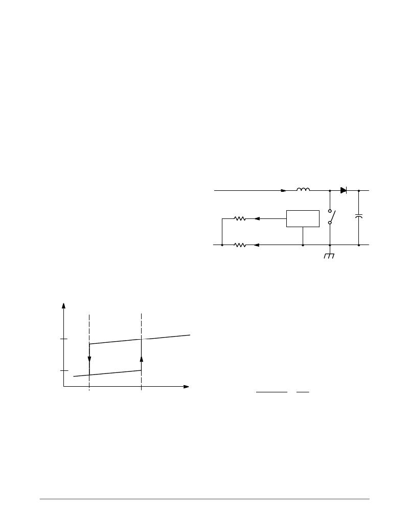
�Current� Sense�
�The� device� senses� the� inductor� current� I� L� by� the� current�
�sense� scheme� in� Figure� 36.� The� device� maintains� the�
�voltage� at� the� CS� pin� (Pin� 4)� to� be� zero� voltage� (i.e.,�
�V� S� ≈� 0� V)� so� that� (eq.10)� can� be� formulated.�
�I� L�
�CS�
�+�
�Gnd�
�R� CS� I� L� ?�
�Figure� 36.� Current� Sensing�
�This� scheme� has� the� advantage� of� the� minimum� number�
�of� components� for� current� sensing� and� the� inrush� current�
�limitation� by� the� resistor� R� CS� .� Hence,� the� sense� current� I� S�
�represents� the� inductor� current� I� L� and� will� be� used� in� the�
�PFC� duty� modulation� to� generate� the� multiplier� voltage�
�V� M� ,� Overpower� Limitation� (OPL),� and� overcurrent�
�protection.�
�I� CC2�
�Shutdown�
�Operating�
�Overcurrent� Protection� (OCP)�
�Overcurrent� protection� is� reached� when� I� S� is� larger� than�
�I� S(OCP)� (200� m� A� typical).� The� offset� voltage� of� the� CS� pin�
�is� typical� 10� mV� and� it� is� neglected� in� the� calculation.�
�12%� I� ref�
�FB�
�ref�
�RSIS(OCP)� RS�
�IL(OCP)� +�
�200� m� A�
�+�
�I� stdn�
�8%� I� I�
�Figure� 35.� Undervoltage� Protection�
�When� the� feedback� current� I� FB� is� less� than� 8%� of� the�
�reference� current� I� ref� (i.e.,� the� output� voltage� V� out� is� less�
�than� 8%� of� its� nominal� value),� the� device� is� shut� down� and�
�consumes� less� than� 50� m� A.� The� device� automatically� starts�
�operation� when� the� output� voltage� goes� above� 12%� of� the�
�nominal� regulation� level.� In� normal� situation� of� boost�
�converter� configuration,� the� output� voltage� V� out� is� always�
�greater� than� the� input� voltage� V� in� and� the� feedback� current�
�I� FB� is� always� greater� than� 8%� and� 12%� of� the� nominal� level�
�Hence,� the� maximum� OCP� inductor� current� threshold�
�I� L(OCP)� is� obtained� in� (eq.15).�
�(eq.18)�
�RCS� RCS�
�When� overcurrent� protection� threshold� is� reached,� the�
�Drive� Output� (Pin� 7)� of� the� device� goes� low.� The� device�
�automatically� resumes� operation� when� the� inductor� current�
�goes� below� the� threshold.�
�Input� Voltage� Sense�
�The� device� senses� the� RMS� input� voltage� V� ac� by� the�
�sensing� scheme� in� Figure� 37.� The� internal� current� mirror� is�
�with� a� typical� 4� V� offset� voltage� at� its� input� so� that� the�
�current� I� vac� can� be� derived� in� (eq.9).� An� external� capacitor�
�C� vac� is� to� maintain� the� In� pin� (Pin� 3)� voltage� in� the�
�http://onsemi.com�
�13�
�相关PDF资料 |
PDF描述 |
|---|---|
| RSC31DRYH-S93 | CONN EDGECARD 62POS DIP .100 SLD |
| VE-J1L-IZ | CONVERTER MOD DC/DC 28V 25W |
| VE-J0Z-IZ | CONVERTER MOD DC/DC 2V 10W |
| NCP1603D100R2 | IC CTRLR PFC/PWM HV START 16SOIC |
| RAC03-12SC | CONV AC/DC 3W 12V OUT SGL T/H |
相关代理商/技术参数 |
参数描述 |
|---|---|
| NCP1653DR2G | 功能描述:功率因数校正 IC Fixed Frequency Current Mode PFC RoHS:否 制造商:Fairchild Semiconductor 开关频率:300 KHz 最大功率耗散: 最大工作温度:+ 125 C 安装风格:SMD/SMT 封装 / 箱体:SOIC-8 封装:Reel |
| NCP1653EVB | 功能描述:BOARD EVAL FOR NCP1653 RoHS:是 类别:编程器,开发系统 >> 评估演示板和套件 系列:- 标准包装:1 系列:PCI Express® (PCIe) 主要目的:接口,收发器,PCI Express 嵌入式:- 已用 IC / 零件:DS80PCI800 主要属性:- 次要属性:- 已供物品:板 |
| NCP1653GEVB | 制造商:ON Semiconductor 功能描述:NCP1653 PFC CCM STEP-UP - Bulk 制造商:ON Semiconductor 功能描述:BOARD EVAL FOR NCP1653 |
| NCP1653P | 功能描述:功率因数校正 IC Fixed Frequency RoHS:否 制造商:Fairchild Semiconductor 开关频率:300 KHz 最大功率耗散: 最大工作温度:+ 125 C 安装风格:SMD/SMT 封装 / 箱体:SOIC-8 封装:Reel |
| NCP1653PG | 功能描述:功率因数校正 IC Fixed Frequency Current Mode PFC RoHS:否 制造商:Fairchild Semiconductor 开关频率:300 KHz 最大功率耗散: 最大工作温度:+ 125 C 安装风格:SMD/SMT 封装 / 箱体:SOIC-8 封装:Reel |
发布紧急采购,3分钟左右您将得到回复。