- 您现在的位置:买卖IC网 > PDF目录22206 > NCP1653DR2 (ON Semiconductor)IC CTRLR PFC CURRENT MODE 8SOIC PDF资料下载
参数资料
| 型号: | NCP1653DR2 |
| 厂商: | ON Semiconductor |
| 文件页数: | 15/19页 |
| 文件大小: | 0K |
| 描述: | IC CTRLR PFC CURRENT MODE 8SOIC |
| 产品变化通告: | LTB Notification 03/Jan/2008 |
| 标准包装: | 1 |
| 模式: | 连续导电(CCM) |
| 频率 - 开关: | 90kHz ~ 110kHz |
| 电源电压: | 8.75 V ~ 18 V |
| 工作温度: | -40°C ~ 125°C |
| 安装类型: | 表面贴装 |
| 封装/外壳: | 8-SOIC(0.154",3.90mm 宽) |
| 供应商设备封装: | 8-SOICN |
| 包装: | 剪切带 (CT) |
| 其它名称: | NCP1653DR2OSCT |
�� �
�
�NCP1653,� NCP1653A�
�V� in�
�C2�
�V� CC�
�C1�
�V� out�
�V� CC� Undervoltage� Lockout� (UVLO)�
�The� device� typically� starts� to� operate� when� the� supply�
�voltage� V� CC� exceeds� 13.25� V.� It� turns� off� when� the� supply�
�voltage� V� CC� goes� below� 8.7� V.� An� 18� V� internal� ESD� Zener�
�Diode� is� connected� to� the� V� CC� pin� (Pin� 8)� to� prevent�
�excessive� supply� voltage.� After� startup,� the� operating� range�
�is� between� 8.7� V� and� 18� V.�
�Thermal� Shutdown�
�An� internal� thermal� circuitry� disables� the� circuit� gate�
�drive� and� then� keeps� the� power� switch� off� when� the� junction�
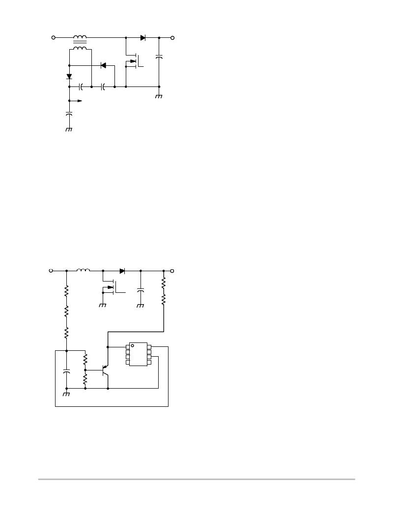
�Figure� 40.� Self� ?� biasing� Scheme� in� Constant� Output�
�Voltage� Mode�
�When� the� NCP1653� circuit� is� required� to� be� startup�
�independently� from� the� second� ?� stage� converter,� it� is�
�recommended� to� use� a� circuit� in� Figure� 41.� When� there� is�
�no� feedback� current� (I� FB� =� 0� m� A)� applied� to� FB� pin� (Pin� 1),�
�the� NCP1653� V� CC� startup� current� is� as� low� (50� m� A�
�maximum).� It� is� good� for� saving� the� current� to� charge� the�
�V� CC� capacitor.� However,� when� there� is� some� feedback�
�current� the� startup� current� rises� to� as� high� as� 1.5� mA� in� the�
�V� CC� <� 4� V� region.� That� is� why� the� circuit� of� Figure� 41� can�
�be� implemented:� a� PNP� bipolar� transistor� derives� the�
�feedback� current� to� ground� at� low� V� CC� levels� (V� CC� <� 4� V)�
�so� that� the� startup� current� keeps� low� and� an� initial� voltage�
�can� be� quickly� built� up� in� the� V� CC� capacitor.� The� values� in�
�Figure� 41� are� just� for� reference.�
�temperature� exceeds� 150� _� C.� The� output� stage� is� then�
�enabled� once� the� temperature� drops� below� typically� 120� _� C�
�(i.e.,� 30� _� C� hysteresis).� The� thermal� shutdown� is� provided�
�to� prevent� possible� device� failures� that� could� result� from� an�
�accidental� overheating.�
�Output� Drive�
�The� output� stage� of� the� device� is� designed� for� direct� drive�
�of� power� MOSFET.� It� is� capable� of� up� to� ±� 1.5� A� peak� drive�
�current� and� has� a� typical� rise� and� fall� time� of� 88� and�
�61.5� ns� with� a� 2.2� nF� load.�
�Input�
�180k�
�180k�
�180k�
�1.5M�
�Output�
�100uF�
�560k�
�BC556�
�NCP1653�
�Figure� 41.� Recommended� Startup� Biasing� Scheme�
�http://onsemi.com�
�15�
�相关PDF资料 |
PDF描述 |
|---|---|
| RSC31DRYH-S93 | CONN EDGECARD 62POS DIP .100 SLD |
| VE-J1L-IZ | CONVERTER MOD DC/DC 28V 25W |
| VE-J0Z-IZ | CONVERTER MOD DC/DC 2V 10W |
| NCP1603D100R2 | IC CTRLR PFC/PWM HV START 16SOIC |
| RAC03-12SC | CONV AC/DC 3W 12V OUT SGL T/H |
相关代理商/技术参数 |
参数描述 |
|---|---|
| NCP1653DR2G | 功能描述:功率因数校正 IC Fixed Frequency Current Mode PFC RoHS:否 制造商:Fairchild Semiconductor 开关频率:300 KHz 最大功率耗散: 最大工作温度:+ 125 C 安装风格:SMD/SMT 封装 / 箱体:SOIC-8 封装:Reel |
| NCP1653EVB | 功能描述:BOARD EVAL FOR NCP1653 RoHS:是 类别:编程器,开发系统 >> 评估演示板和套件 系列:- 标准包装:1 系列:PCI Express® (PCIe) 主要目的:接口,收发器,PCI Express 嵌入式:- 已用 IC / 零件:DS80PCI800 主要属性:- 次要属性:- 已供物品:板 |
| NCP1653GEVB | 制造商:ON Semiconductor 功能描述:NCP1653 PFC CCM STEP-UP - Bulk 制造商:ON Semiconductor 功能描述:BOARD EVAL FOR NCP1653 |
| NCP1653P | 功能描述:功率因数校正 IC Fixed Frequency RoHS:否 制造商:Fairchild Semiconductor 开关频率:300 KHz 最大功率耗散: 最大工作温度:+ 125 C 安装风格:SMD/SMT 封装 / 箱体:SOIC-8 封装:Reel |
| NCP1653PG | 功能描述:功率因数校正 IC Fixed Frequency Current Mode PFC RoHS:否 制造商:Fairchild Semiconductor 开关频率:300 KHz 最大功率耗散: 最大工作温度:+ 125 C 安装风格:SMD/SMT 封装 / 箱体:SOIC-8 封装:Reel |
发布紧急采购,3分钟左右您将得到回复。