- 您现在的位置:买卖IC网 > PDF目录22206 > NCP1653DR2 (ON Semiconductor)IC CTRLR PFC CURRENT MODE 8SOIC PDF资料下载
参数资料
| 型号: | NCP1653DR2 |
| 厂商: | ON Semiconductor |
| 文件页数: | 3/19页 |
| 文件大小: | 0K |
| 描述: | IC CTRLR PFC CURRENT MODE 8SOIC |
| 产品变化通告: | LTB Notification 03/Jan/2008 |
| 标准包装: | 1 |
| 模式: | 连续导电(CCM) |
| 频率 - 开关: | 90kHz ~ 110kHz |
| 电源电压: | 8.75 V ~ 18 V |
| 工作温度: | -40°C ~ 125°C |
| 安装类型: | 表面贴装 |
| 封装/外壳: | 8-SOIC(0.154",3.90mm 宽) |
| 供应商设备封装: | 8-SOICN |
| 包装: | 剪切带 (CT) |
| 其它名称: | NCP1653DR2OSCT |
�� �
�
�NCP1653,� NCP1653A�
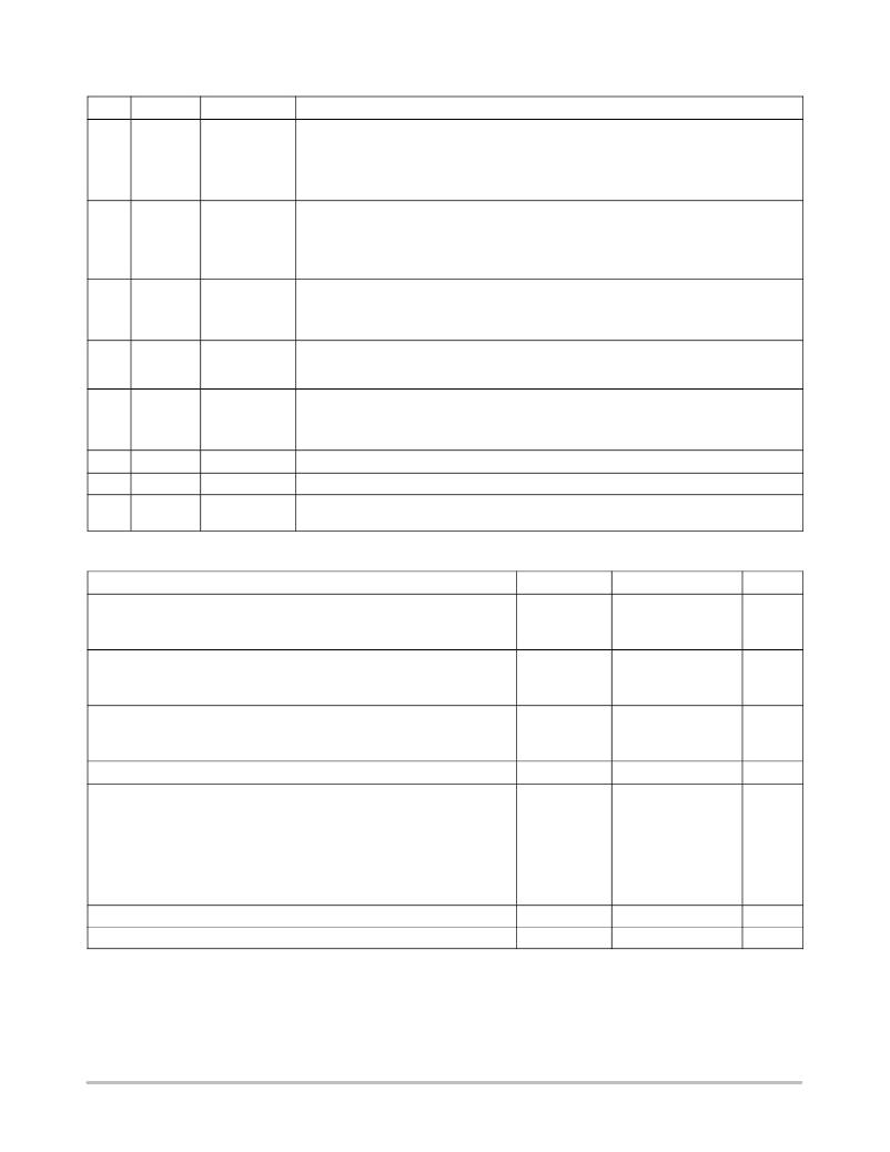
�PIN� FUNCTION� DESCRIPTION�
�Pin�
�1�
�Symbol�
�FB� /� SD�
�Name�
�Feedback� /�
�Shutdown�
�Function�
�This� pin� receives� a� feedback� current� I� FB� which� is� proportional� to� the� PFC� circuit� output� voltage.�
�The� current� is� for� output� regulation,� output� overvoltage� protection� (OVP),� and� output� undervoltage�
�protection� (UVP).�
�When� I� FB� goes� above� 107%� I� ref� ,� OVP� is� activated� and� the� Drive� Output� is� disabled.�
�When� I� FB� goes� below� 8%� I� ref� ,� the� device� enters� a� low� ?� consumption� shutdown� mode.�
�2�
�V� control�
�Control� Voltage� /�
�Soft� ?� Start�
�The� voltage� of� this� pin� V� control� directly� controls� the� input� impedance� and� hence� the� power� factor� of�
�the� circuit.� This� pin� is� connected� to� an� external� capacitor� C� control� to� limit� the� V� control� bandwidth�
�typically� below� 20� Hz� to� achieve� near� unity� power� factor.�
�The� device� provides� no� output� when� V� control� =� 0� V.� Hence,� C� control� also� works� as� a� soft� ?� start�
�capacitor.�
�3�
�4�
�5�
�6�
�7�
�8�
�In�
�CS�
�V� M�
�GND�
�Drv�
�V� CC�
�Input� Voltage�
�Sense�
�Input� Current�
�Sense�
�Multiplier�
�Voltage�
�The� IC� Ground�
�Drive� Output�
�Supply� Voltage�
�This� pin� sinks� an� input� ?� voltage� current� I� vac� which� is� proportional� to� the� RMS� input� voltage� V� ac� .�
�The� current� I� vac� is� for� overpower� limitation� (OPL)� and� PFC� duty� cycle� modulation.� When� the�
�product� (I� S� ?� I� vac� )� goes� above� 3� nA� 2� ,� OPL� is� activated� and� the� Drive� Output� duty� ratio� is� reduced� by�
�pulling� down� V� control� indirectly� to� reduce� the� input� power.�
�This� pin� sources� a� current� I� S� which� is� proportional� to� the� inductor� current� I� L� .� The� sense� current� I� S�
�is� for� overcurrent� protection� (OCP),� overpower� limitation� (OPL)� and� PFC� duty� cycle� modulation.�
�When� I� S� goes� above� 200� m� A,� OCP� is� activated� and� the� Drive� Output� is� disabled.�
�This� pin� provides� a� voltage� V� M� for� the� PFC� duty� cycle� modulation.� The� input� impedance� of� the�
�PFC� circuit� is� proportional� to� the� resistor� R� M� externally� connected� to� this� pin.� The� device� operates�
�in� average� current� ?� mode� if� an� external� capacitor� C� M� is� connected� to� the� pin.� Otherwise,� it�
�operates� in� peak� current� ?� mode.�
�?�
�This� pin� provides� an� output� to� an� external� MOSFET.�
�This� pin� is� the� positive� supply� of� the� device.� The� operating� range� is� between� 8.75� V� and� 18� V� with�
�UVLO� start� threshold� 13.25� V.�
�MAXIMUM� RATINGS�
�Rating�
�Symbol�
�Value�
�Unit�
�FB,� V� control� ,� In,� CS,� V� M� Pins� (Pins� 1� ?� 5)�
�Maximum� Voltage� Range�
�Maximum� Current�
�V� max�
�I� max�
�?� 0.3� to� +9�
�100�
�V�
�mA�
�Drive� Output� (Pin� 7)�
�Maximum� Voltage� Range�
�Maximum� Current� Range� (Note� 1)�
�V� max�
�I� max�
�?� 0.3� to� +18�
�1.5�
�V�
�A�
�Power� Supply� Voltage� (Pin� 8)�
�Maximum� Voltage� Range�
�Maximum� Current�
�Transient� Power� Supply� Voltage,� Duration� <� 10� ms,� IV� CC� <� 20� mA�
�V� max�
�I� max�
�?� 0.3� to� +18�
�100�
�25�
�V�
�mA�
�V�
�Power� Dissipation� and� Thermal� Characteristics�
�P� suffix,� Plastic� Package,� Case� 626�
�Maximum� Power� Dissipation� @� T� A� =� 70� °� C�
�Thermal� Resistance� Junction� ?� to� ?� Air�
�D� suffix,� Plastic� Package,� Case� 751�
�Maximum� Power� Dissipation� @� T� A� =� 70� °� C�
�Thermal� Resistance� Junction� ?� to� ?� Air�
�Operating� Junction� Temperature� Range�
�Storage� Temperature� Range�
�P� D�
�R� q� JA�
�P� D�
�R� q� JA�
�T� J�
�T� stg�
�800�
�100�
�450�
�178�
�?� 40� to� +125�
�?� 65� to� +150�
�mW�
�°� C/W�
�mW�
�°� C/W�
�°� C�
�°� C�
�Stresses� exceeding� Maximum� Ratings� may� damage� the� device.� Maximum� Ratings� are� stress� ratings� only.� Functional� operation� above� the�
�Recommended� Operating� Conditions� is� not� implied.� Extended� exposure� to� stresses� above� the� Recommended� Operating� Conditions� may� affect�
�device� reliability.�
�A.� This� device� series� contains� ESD� protection� and� exceeds� the� following� tests:�
�Pins� 1� ?� 8:� Human� Body� Model� 2000� V� per� MIL� ?� STD� ?� 883,� Method� 3015.�
�Machine� Model� Method� 190� V.�
�B.� This� device� contains� Latchup� protection� and� exceeds� ±� 100� mA� per� JEDEC� Standard� JESD78.�
�1.� Guaranteed� by� design.�
�http://onsemi.com�
�3�
�相关PDF资料 |
PDF描述 |
|---|---|
| RSC31DRYH-S93 | CONN EDGECARD 62POS DIP .100 SLD |
| VE-J1L-IZ | CONVERTER MOD DC/DC 28V 25W |
| VE-J0Z-IZ | CONVERTER MOD DC/DC 2V 10W |
| NCP1603D100R2 | IC CTRLR PFC/PWM HV START 16SOIC |
| RAC03-12SC | CONV AC/DC 3W 12V OUT SGL T/H |
相关代理商/技术参数 |
参数描述 |
|---|---|
| NCP1653DR2G | 功能描述:功率因数校正 IC Fixed Frequency Current Mode PFC RoHS:否 制造商:Fairchild Semiconductor 开关频率:300 KHz 最大功率耗散: 最大工作温度:+ 125 C 安装风格:SMD/SMT 封装 / 箱体:SOIC-8 封装:Reel |
| NCP1653EVB | 功能描述:BOARD EVAL FOR NCP1653 RoHS:是 类别:编程器,开发系统 >> 评估演示板和套件 系列:- 标准包装:1 系列:PCI Express® (PCIe) 主要目的:接口,收发器,PCI Express 嵌入式:- 已用 IC / 零件:DS80PCI800 主要属性:- 次要属性:- 已供物品:板 |
| NCP1653GEVB | 制造商:ON Semiconductor 功能描述:NCP1653 PFC CCM STEP-UP - Bulk 制造商:ON Semiconductor 功能描述:BOARD EVAL FOR NCP1653 |
| NCP1653P | 功能描述:功率因数校正 IC Fixed Frequency RoHS:否 制造商:Fairchild Semiconductor 开关频率:300 KHz 最大功率耗散: 最大工作温度:+ 125 C 安装风格:SMD/SMT 封装 / 箱体:SOIC-8 封装:Reel |
| NCP1653PG | 功能描述:功率因数校正 IC Fixed Frequency Current Mode PFC RoHS:否 制造商:Fairchild Semiconductor 开关频率:300 KHz 最大功率耗散: 最大工作温度:+ 125 C 安装风格:SMD/SMT 封装 / 箱体:SOIC-8 封装:Reel |
发布紧急采购,3分钟左右您将得到回复。