- 您现在的位置:买卖IC网 > PDF目录20421 > NCP1654PFCGEVB (ON Semiconductor)EVAL BOARD FOR NCP1654PFCG PDF资料下载
参数资料
| 型号: | NCP1654PFCGEVB |
| 厂商: | ON Semiconductor |
| 文件页数: | 13/23页 |
| 文件大小: | 228K |
| 描述: | EVAL BOARD FOR NCP1654PFCG |
| 设计资源: | NCP1654EVB BOM NCP1654EVB Gerber Files NCP1654EVB Schematic |
| 标准包装: | 1 |
| 主要目的: | AC/DC,次级 |
| 输出及类型: | 1,非隔离 |
| 输出电压: | 378 ~ 401 V |
| 输入电压: | 85 ~ 230 VAC,15VDC |
| 稳压器拓扑结构: | 升压 |
| 频率 - 开关: | 65kHz |
| 板类型: | 完全填充 |
| 已供物品: | 板 |
| 已用 IC / 零件: | NCP1654 |
| 其它名称: | NCP1654PFCGEVBOS |
NCP1654
http://onsemi.com
13
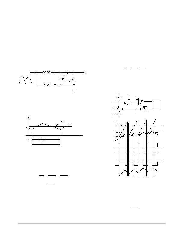
PRINCIPLE OF NCP1654 SCHEME
CCM PFC Boost
A CCM PFC boost converter is shown in Figure 31. The
input voltage is a rectified 50 ro 60 Hz sinusoidal signal.
The MOSFET is switching at a high frequency (typically
65/133/200 kHz in NCP1654) so that the inductor current
I
L
basically consists of high and lowfrequency
components.
Filter capacitor C
filter
is an essential and very small value
capacitor in order to eliminate the highfrequency
component of the inductor I
L
. This filter capacitor cannot
be too bulky because it can pollute the power factor by
distorting the rectified sinusoidal input voltage.
Figure 31. CCM PFC Boost Converter
+
C
bulk
V
in
R
SENSE
C
filter
L
I
in
I
L
V
out
Output
Voltage
PFC Methodology
The NCP1654 uses a proprietary PFC methodology
particularly designed for CCM operation. The PFC
methodology is described in this section.
Figure 32. Inductor Current in CCM
Time
I
in
I
L
t
1
t
2
T
As shown in Figure 32, the inductor current I
L
in a
switching period T includes a charging phase for duration
t
1
and a discharging phase for duration t
2
. The voltage
conversion ratio is obtained in (Equation 1).
V
out
V
in
+
t
1
) t
2
t
2
+
T
T * t
1
(eq. 1)
V
in
+
T * t
1
T
V
out
where
V
out
is the output voltage of PFC stage,
V
in
is the rectified input voltage,
T is the switching period,
t
1
is the MOSFET on time, and
t
2
is the MOSFET off time.
The input filter capacitor C
filter
and the frontended EMI
filter absorbs the highfrequency component of inductor
current I
L
. It makes the input current I
in
a lowfrequency
signal only of the inductor current.
(eq. 2)
I
in
+ I
L*50
where
I
in
is the input AC current.
I
L
is the inductor current.
I
L50
supposes a 50 Hz operation. The suffix 50 means
it is with a 50 Hz bandwidth of the original I
L
.
From (Equation 1) and (Equation 2), the input
impedance Z
in
is formulated.
(eq. 3)
Z
in
+
V
in
I
in
+
T * t
1
T
V
out
I
L*50
where Z
in
is input impedance.
Power factor is corrected when the input impedance Z
in
in (Equation 3) is constant or varies slowly in the 50 or 60
Hz bandwidth.
Figure 33. PFC Duty Modulation and Timing Diagram
+
-
+
I
ch
V
M
V
ref
PFC Modulation
V
ramp
C
ramp
R
S
Q
Clock
0
1
V
ramp
V
ref
V
M
V
M
without
Filtering
Clock
Latch Set
Latch Reset
Output
Inductor
Current
The PFC modulation and timing diagram is shown in
Figure 33. The MOSFET on time t
1
is generated by the
intersection of reference voltage V
REF
and ramp voltage
V
ramp
. A relationship in (Equation 4) is obtained.
(eq. 4)
V
ramp
+ V
m
)
I
ch
t
1
C
ramp
+ V
REF
where
相关PDF资料 |
PDF描述 |
|---|---|
| EGM08DTKN | CONN EDGECARD 16POS DIP .156 SLD |
| ESC06DRXN-S734 | CONN EDGECARD 12POS DIP .100 SLD |
| VE-B3R-CX-F3 | CONVERTER MOD DC/DC 7.5V 75W |
| VE-B3R-CX-F1 | CONVERTER MOD DC/DC 7.5V 75W |
| SDR0403-300JL | INDUCTOR 30UH 5% NON-SHLD SMD |
相关代理商/技术参数 |
参数描述 |
|---|---|
| NCP1729-SKT | 制造商:P&S 功能描述:Sample Kit, including Two NCP1729SN35T1 and A Development Source CD-ROM 制造商:P&S 功能描述:Sample Kit,including Two NCP1729SN35T1 and A Development Source CD-ROM |
| NCP1729SN35T1 | 功能描述:电荷泵 Switched Cap Voltage RoHS:否 制造商:Maxim Integrated 功能:Inverting, Step Up 输出电压:- 1.5 V to - 5.5 V, 3 V to 11 V 输出电流:100 mA 电源电流:1 mA 最大工作温度:+ 70 C 封装 / 箱体:SOIC-8 Narrow 封装:Tube |
| NCP1729SN35T1G | 功能描述:电荷泵 Switched Cap Voltage Inverter w/Shutdown RoHS:否 制造商:Maxim Integrated 功能:Inverting, Step Up 输出电压:- 1.5 V to - 5.5 V, 3 V to 11 V 输出电流:100 mA 电源电流:1 mA 最大工作温度:+ 70 C 封装 / 箱体:SOIC-8 Narrow 封装:Tube |
| NCP1729SN35T1G | 制造商:ON Semiconductor 功能描述:Power Supply IC |
| NCP1800DM41R2 | 功能描述:电池管理 4.1V Single Cell RoHS:否 制造商:Texas Instruments 电池类型:Li-Ion 输出电压:5 V 输出电流:4.5 A 工作电源电压:3.9 V to 17 V 最大工作温度:+ 85 C 最小工作温度:- 40 C 封装 / 箱体:VQFN-24 封装:Reel |
发布紧急采购,3分钟左右您将得到回复。