- 您现在的位置:买卖IC网 > PDF目录20421 > NCP1654PFCGEVB (ON Semiconductor)EVAL BOARD FOR NCP1654PFCG PDF资料下载
参数资料
| 型号: | NCP1654PFCGEVB |
| 厂商: | ON Semiconductor |
| 文件页数: | 19/23页 |
| 文件大小: | 228K |
| 描述: | EVAL BOARD FOR NCP1654PFCG |
| 设计资源: | NCP1654EVB BOM NCP1654EVB Gerber Files NCP1654EVB Schematic |
| 标准包装: | 1 |
| 主要目的: | AC/DC,次级 |
| 输出及类型: | 1,非隔离 |
| 输出电压: | 378 ~ 401 V |
| 输入电压: | 85 ~ 230 VAC,15VDC |
| 稳压器拓扑结构: | 升压 |
| 频率 - 开关: | 65kHz |
| 板类型: | 完全填充 |
| 已供物品: | 板 |
| 已用 IC / 零件: | NCP1654 |
| 其它名称: | NCP1654PFCGEVBOS |
NCP1654
http://onsemi.com
19
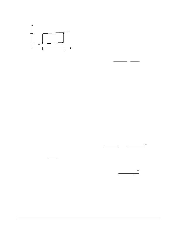
Undervoltage Protection (UVP) for Open Loop
Protection or Shutdown
Figure 44. Undervoltage Protection
I
STDN
I
CC2
Shutdown
Operating
8% V
REF
12% V
REF
V
fb
As shown in Figure 44, when V
fb
is less than 8% of V
REF
,
the device is shut down and consumes less than 400 mA.
The device automatically starts operation when the output
voltage goes above 12% of V
REF
. In normal situation of
boost converter configuration, the output voltage V
out
is
always greater than the input voltage V
in
and the feedback
signal V
fb
is always greater than 8% and 12% of V
REF
to
enable NCP1654 to operate.
This Undervoltage Protection function has 2 purposes.
" Open Loop Protection Protect the power stage from
damage at feedback loop abnormal, such as V
fb
is
shorted to ground or the feedback resistor R
fbU
is
open.
" Shutdown mode Disables the PFC stage and forces a
low consumption mode. This feature helps to meet
stringent standby specifications. Power Factor being
not necessary in standby, the PFC stage is generally
inhibited to save the preconverter losses. To further
improve the standby performance, the PFC controller
should consume minimum current in this mode.
Current Sense
The device senses the inductor current I
L
by the current
sense scheme in Figure 37. The device maintains the
voltage at CS pin to be zero voltage (i.e., V
cs
H 0 V) so that
(Equation 11),
I
cs
+
R
SENSE
R
CS
I
L
,
can be formulated.
This scheme has the advantage of the minimum number
of components for current sensing. The sense current I
cs
represents the inductor current I
L
and will be used in the
PFC duty modulation to generate the multiplier voltage
V
m
, OverPower Limitation (OPL), and OverCurrent
Protection. (Equation 11) would insist in the fact that it
provides the flexibility in the R
SENSE
choice and that it
allows to detect inrush currents.
OverCurrent Protection (OCP)
OverCurrent Protection is reached when I
cs
is larger
than I
S(OCP)
(200 mA typical). The offset voltage of the CS
pin is typical 10 mV and it is neglected in the calculation.
Hence, the maximum OCP inductor current threshold
I
L(OCP)
is obtained in (Equation 20).
(eq. 20)
I
L(OCP)
+
R
CS
I
S(OCP)
R
SENSE
+
R
CS
R
SENSE
@ 200 mA
When overcurrent protection threshold is reached, the
Drive Output of the device goes low. The device
automatically resumes operation when the inductor current
goes below the threshold.
Input Voltage Sense
The device senses the rms input voltage V
ac
by the
sensing scheme in Figure 45. V
bo
senses the average
rectified input voltage V
in
via the resistor divider. An
external capacitor C
BO
is to maintain the V
bo
the average
value of V
in
. V
bo
is used for BrownOut Protection, PFC
duty modulation and overpower limitation (OPL).
BrownOut Protection
The device uses the V
bo
signal to protect the PFC stage
from operating as the input voltage is lower than expected.
Reformulate (Equation 9) to get (Equation 21). Refer to
Figure 45, V
in
is different before and after the device
operating.
" Before the device operates, V
in
is equal to the peak
value of rms input voltage, V
ac
. Hence V
bo
is as
described in (Equation 21).
(eq. 21)
V
bo
+
R
boL
R
boL
) R
boU
(V
in
) +
R
boL
R
boL
) R
boU
2
V
ac
" After device operates, V
in
is the rectified sinusoidal
input voltage. Thanks to C
BO
, V
bo
is the average of
rectified input voltage. Hence V
bo
decays to 2/p of the
peak value of rms input voltage V
ac
as described in
(Equation 22).
(eq. 22)
V
bo
+
R
boL
R
boL
) R
boU
2 2
p
V
ac
相关PDF资料 |
PDF描述 |
|---|---|
| EGM08DTKN | CONN EDGECARD 16POS DIP .156 SLD |
| ESC06DRXN-S734 | CONN EDGECARD 12POS DIP .100 SLD |
| VE-B3R-CX-F3 | CONVERTER MOD DC/DC 7.5V 75W |
| VE-B3R-CX-F1 | CONVERTER MOD DC/DC 7.5V 75W |
| SDR0403-300JL | INDUCTOR 30UH 5% NON-SHLD SMD |
相关代理商/技术参数 |
参数描述 |
|---|---|
| NCP1729-SKT | 制造商:P&S 功能描述:Sample Kit, including Two NCP1729SN35T1 and A Development Source CD-ROM 制造商:P&S 功能描述:Sample Kit,including Two NCP1729SN35T1 and A Development Source CD-ROM |
| NCP1729SN35T1 | 功能描述:电荷泵 Switched Cap Voltage RoHS:否 制造商:Maxim Integrated 功能:Inverting, Step Up 输出电压:- 1.5 V to - 5.5 V, 3 V to 11 V 输出电流:100 mA 电源电流:1 mA 最大工作温度:+ 70 C 封装 / 箱体:SOIC-8 Narrow 封装:Tube |
| NCP1729SN35T1G | 功能描述:电荷泵 Switched Cap Voltage Inverter w/Shutdown RoHS:否 制造商:Maxim Integrated 功能:Inverting, Step Up 输出电压:- 1.5 V to - 5.5 V, 3 V to 11 V 输出电流:100 mA 电源电流:1 mA 最大工作温度:+ 70 C 封装 / 箱体:SOIC-8 Narrow 封装:Tube |
| NCP1729SN35T1G | 制造商:ON Semiconductor 功能描述:Power Supply IC |
| NCP1800DM41R2 | 功能描述:电池管理 4.1V Single Cell RoHS:否 制造商:Texas Instruments 电池类型:Li-Ion 输出电压:5 V 输出电流:4.5 A 工作电源电压:3.9 V to 17 V 最大工作温度:+ 85 C 最小工作温度:- 40 C 封装 / 箱体:VQFN-24 封装:Reel |
发布紧急采购,3分钟左右您将得到回复。