- 您现在的位置:买卖IC网 > PDF目录20421 > NCP1654PFCGEVB (ON Semiconductor)EVAL BOARD FOR NCP1654PFCG PDF资料下载
参数资料
| 型号: | NCP1654PFCGEVB |
| 厂商: | ON Semiconductor |
| 文件页数: | 14/23页 |
| 文件大小: | 228K |
| 描述: | EVAL BOARD FOR NCP1654PFCG |
| 设计资源: | NCP1654EVB BOM NCP1654EVB Gerber Files NCP1654EVB Schematic |
| 标准包装: | 1 |
| 主要目的: | AC/DC,次级 |
| 输出及类型: | 1,非隔离 |
| 输出电压: | 378 ~ 401 V |
| 输入电压: | 85 ~ 230 VAC,15VDC |
| 稳压器拓扑结构: | 升压 |
| 频率 - 开关: | 65kHz |
| 板类型: | 完全填充 |
| 已供物品: | 板 |
| 已用 IC / 零件: | NCP1654 |
| 其它名称: | NCP1654PFCGEVBOS |
NCP1654
http://onsemi.com
14
V
ramp
is the internal ramp voltage, the positive input of the
PFC modulation comparator,
V
m
is the multiplier voltage appearing on V
m
pin,
I
ch
is the internal charging current,
C
ramp
is the internal ramp capacitor, and
V
REF
is the internal reference voltage, the negative input of
the PFC modulation comparator.
I
ch
, C
ramp
, and V
REF
also act as the ramp signal of
switching frequency. Hence the charging current I
ch
is
specially designed as in (Equation 5). The multiplier
voltage V
m
is therefore expressed in terms of t
1
in
(Equation 6).
(eq. 5)
I
ch
+
C
ramp
V
REF
T
(eq. 6)
V
m
+ V
REF
*
t
1
C
ram
C
ramp
V
REF
T
+ V
REF
T * t
1
T
From (Equation 3) and (Equation 6), the input impedance
Z
in
is reformulated in (Equation 7).
(eq. 7)
Z
in
+
V
m
V
REF
V
out
I
L*50
Because V
REF
and V
out
are roughly constant versus time,
the multiplier voltage V
m
is designed to be proportional to
the I
L50
in order to have a constant Z
in
for PFC purpose.
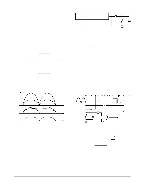
It is illustrated in Figure 34.
Figure 34. Multiplier Voltage Timing Diagram
Time
Time
Time
V
M
I
L
I
in
V
in
It can be seen in the timing diagram in Figure 33 that V
m
originally consists of a switching frequency ripple coming
from the inductor current I
L
. The duty ratio can be
inaccurately generated due to this ripple. This modulation
is the socalled
peak current mode
. Hence, an external
capacitor C
M
connected to the multiplier voltage V
m
pin is
essential to bypass the highfrequency component of V
m
.
The modulation becomes the socalled
average current
mode
with a better accuracy for PFC.
Figure 35. External Connection on the Multiplier
Voltage Pin
PFC Duty
Modulation
V
m
+
R
M
I
cs
V
bo
4(V
control
* V
CONTROL(min)
)
R
M
C
M
V
m
I
m
2
The multiplier voltage V
m
is generated according to
(Equation 8).
(eq. 8)
V
m
+
R
M
I
cs
V
bo
4(V
control
* V
CONTROL(min)
)
Where,
R
M
is the external multiplier resistor connected to V
m
pin,
which is constant.
V
bo
is the input voltage signal appearing on the BO pin,
which is proportional to the rms input voltage,
I
cs
is the sense current proportional to the inductor current
I
L
as described in (Equation 11).
V
control
is the control voltage signal, the output voltage of
Operational Transconductance Amplifier (OTA), as
described in (Equation 12).
R
M
directly limits the maximum input power capability
and hence its value affects the NCP1654 to operate in either
follower boost mode
or
constant output voltage mode
.
Figure 36. External Connection on the Brown Out Pin
Vbo
BO
4
+
R
boL
V
in
R
boU
C
BO
+
-
V
boH
/ V
boL
V
boH
= 1.3 V, V
boL
= 0.7 V
Refer to Figure 36,
(eq. 9)
V
bo
+ K
BO
(V
in
) + K
BO
@
2 2
p
V
ac
(eq. 10)
K
BO
+
R
boL
R
boU
) R
boL
where
V
bo
is the voltage on BO pin.
K
BO
is the decay ratio of V
in
to V
bo
.
<V
in
> is the average voltage signal of V
in
, the voltage
appearing on C
filter
.
V
ac
is the RMS input voltage.
相关PDF资料 |
PDF描述 |
|---|---|
| EGM08DTKN | CONN EDGECARD 16POS DIP .156 SLD |
| ESC06DRXN-S734 | CONN EDGECARD 12POS DIP .100 SLD |
| VE-B3R-CX-F3 | CONVERTER MOD DC/DC 7.5V 75W |
| VE-B3R-CX-F1 | CONVERTER MOD DC/DC 7.5V 75W |
| SDR0403-300JL | INDUCTOR 30UH 5% NON-SHLD SMD |
相关代理商/技术参数 |
参数描述 |
|---|---|
| NCP1729-SKT | 制造商:P&S 功能描述:Sample Kit, including Two NCP1729SN35T1 and A Development Source CD-ROM 制造商:P&S 功能描述:Sample Kit,including Two NCP1729SN35T1 and A Development Source CD-ROM |
| NCP1729SN35T1 | 功能描述:电荷泵 Switched Cap Voltage RoHS:否 制造商:Maxim Integrated 功能:Inverting, Step Up 输出电压:- 1.5 V to - 5.5 V, 3 V to 11 V 输出电流:100 mA 电源电流:1 mA 最大工作温度:+ 70 C 封装 / 箱体:SOIC-8 Narrow 封装:Tube |
| NCP1729SN35T1G | 功能描述:电荷泵 Switched Cap Voltage Inverter w/Shutdown RoHS:否 制造商:Maxim Integrated 功能:Inverting, Step Up 输出电压:- 1.5 V to - 5.5 V, 3 V to 11 V 输出电流:100 mA 电源电流:1 mA 最大工作温度:+ 70 C 封装 / 箱体:SOIC-8 Narrow 封装:Tube |
| NCP1729SN35T1G | 制造商:ON Semiconductor 功能描述:Power Supply IC |
| NCP1800DM41R2 | 功能描述:电池管理 4.1V Single Cell RoHS:否 制造商:Texas Instruments 电池类型:Li-Ion 输出电压:5 V 输出电流:4.5 A 工作电源电压:3.9 V to 17 V 最大工作温度:+ 85 C 最小工作温度:- 40 C 封装 / 箱体:VQFN-24 封装:Reel |
发布紧急采购,3分钟左右您将得到回复。