- 您现在的位置:买卖IC网 > PDF目录20421 > NCP1654PFCGEVB (ON Semiconductor)EVAL BOARD FOR NCP1654PFCG PDF资料下载
参数资料
| 型号: | NCP1654PFCGEVB |
| 厂商: | ON Semiconductor |
| 文件页数: | 17/23页 |
| 文件大小: | 228K |
| 描述: | EVAL BOARD FOR NCP1654PFCG |
| 设计资源: | NCP1654EVB BOM NCP1654EVB Gerber Files NCP1654EVB Schematic |
| 标准包装: | 1 |
| 主要目的: | AC/DC,次级 |
| 输出及类型: | 1,非隔离 |
| 输出电压: | 378 ~ 401 V |
| 输入电压: | 85 ~ 230 VAC,15VDC |
| 稳压器拓扑结构: | 升压 |
| 频率 - 开关: | 65kHz |
| 板类型: | 完全填充 |
| 已供物品: | 板 |
| 已用 IC / 零件: | NCP1654 |
| 其它名称: | NCP1654PFCGEVBOS |
NCP1654
http://onsemi.com
17
The feedback signal V
fb
represents the output voltage
V
out
and will be used in the output voltage regulation,
Overvoltage protection (OVP), fast transient response, and
Undervoltage protection (UVP)
Output Voltage Regulation
NCP1654 uses a high gain Operational Trans
conductance Amplifier (OTA) as error amplifier. Refer to
Figure 38, the output of OTA V
control
operating range is
from V
CONTROL(min)
to V
CONTROL(max)
.
Fast Transient Response
Given the low bandwidth of the regulation block, the
output voltage of PFC stages may exhibit excessive over or
undershoots because of abrupt load or input voltage
variations (such as startup duration). As shown in
Figure 40, if the output voltage is out of regulation,
NCP1654 has 2 functions to maintain the output voltage
regulation.
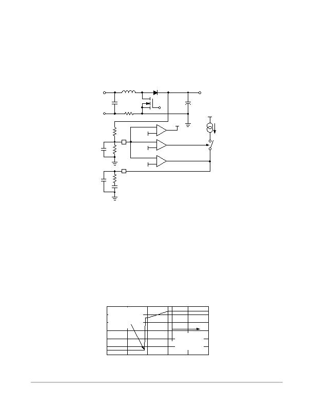
Figure 40. OVP and Fast Transient Response
+
-
+
-
95%
V
REF
V
REF
OTA
6
5
V
control
V
out
Low Detect
200 mA
Vdd
?0 mA
+
-
105%
V
REF
V
out
+
OVP
V
fb
R
fbU
R
fbL
C
FB
" Overvoltage Protection: When V
fb
is higher than
105% of V
REF
(i.e. V
out
> 105% of nominal output
voltage), the Driver output of the device goes low for
protection. The circuit automatically resumes
operation when V
fb
becomes lower than 105% of
V
REF
. If the nominal V
out
is set at 390 V, then the
maximum output voltage is 105% of 390 V = 410 V.
Hence a cost & size effective bulk capacitor of lower
voltage rating is suitable for this application,
" Dynamic response enhancer: NCP1654 drastically
speeds up the regulation loop by its internal 200 mA
enhanced current source when the output voltage is
below 95% of its regulation level. Under normal
condition, the maximum sink and source of output
current capability of OTA is around 28 mA. Thanks to
the
V
out
low detect
block, when the V
fb
is below
95% V
REF
, an extra 200 mA current source will raise
V
control
rapidly. Hence prevent the PFC output from
dropping too low and improve the transient response
performance. The relationship between current
flowing in/out V
control
pin and V
fb
is as shown in
Figure 41.
It is recommended to add a typical 100 pF capacitor C
FB
decoupling capacitor next to feedback pin to prevent from
noise impact.
250
200
150
100
50
0
50
2
2.2
2.4
2.6
2.8
3
Vfb
Figure 41. V
fb
vs. Current Flowing in/out from V
control
Pin
No DRV when
V
fb
is above
105% V
REF
200 mA raises
V
control
rapidly
when V
fb
is below
95% V
REF
相关PDF资料 |
PDF描述 |
|---|---|
| EGM08DTKN | CONN EDGECARD 16POS DIP .156 SLD |
| ESC06DRXN-S734 | CONN EDGECARD 12POS DIP .100 SLD |
| VE-B3R-CX-F3 | CONVERTER MOD DC/DC 7.5V 75W |
| VE-B3R-CX-F1 | CONVERTER MOD DC/DC 7.5V 75W |
| SDR0403-300JL | INDUCTOR 30UH 5% NON-SHLD SMD |
相关代理商/技术参数 |
参数描述 |
|---|---|
| NCP1729-SKT | 制造商:P&S 功能描述:Sample Kit, including Two NCP1729SN35T1 and A Development Source CD-ROM 制造商:P&S 功能描述:Sample Kit,including Two NCP1729SN35T1 and A Development Source CD-ROM |
| NCP1729SN35T1 | 功能描述:电荷泵 Switched Cap Voltage RoHS:否 制造商:Maxim Integrated 功能:Inverting, Step Up 输出电压:- 1.5 V to - 5.5 V, 3 V to 11 V 输出电流:100 mA 电源电流:1 mA 最大工作温度:+ 70 C 封装 / 箱体:SOIC-8 Narrow 封装:Tube |
| NCP1729SN35T1G | 功能描述:电荷泵 Switched Cap Voltage Inverter w/Shutdown RoHS:否 制造商:Maxim Integrated 功能:Inverting, Step Up 输出电压:- 1.5 V to - 5.5 V, 3 V to 11 V 输出电流:100 mA 电源电流:1 mA 最大工作温度:+ 70 C 封装 / 箱体:SOIC-8 Narrow 封装:Tube |
| NCP1729SN35T1G | 制造商:ON Semiconductor 功能描述:Power Supply IC |
| NCP1800DM41R2 | 功能描述:电池管理 4.1V Single Cell RoHS:否 制造商:Texas Instruments 电池类型:Li-Ion 输出电压:5 V 输出电流:4.5 A 工作电源电压:3.9 V to 17 V 最大工作温度:+ 85 C 最小工作温度:- 40 C 封装 / 箱体:VQFN-24 封装:Reel |
发布紧急采购,3分钟左右您将得到回复。