- 您现在的位置:买卖IC网 > Datasheet目录996 > NCP3066SCBCKGEVB (ON Semiconductor)EVAL BOARD FOR NCP3066SCBCKG Datasheet资料下载
参数资料
| 型号: | NCP3066SCBCKGEVB |
| 厂商: | ON Semiconductor |
| 文件页数: | 3/20页 |
| 文件大小: | 0K |
| 描述: | EVAL BOARD FOR NCP3066SCBCKG |
| 设计资源: | NCP3066 Buck SOIC EVB BOM NCP3066SCBCKGEVB Gerber Files NCP3066 BUCK EVB Schematic |
| 标准包装: | 1 |
| 电流 - 输出 / 通道: | 150mA |
| 输出及类型: | 1,非隔离 |
| 输出电压: | 3.2V |
| 特点: | 亮度控制 |
| 输入电压: | 12V |
| 已供物品: | 板 |
| 已用 IC / 零件: | NCP3066 |
| 其它名称: | NCP3066SCBCKGEVBOS |
�� �
�
�NCP3066,� NCV3066�
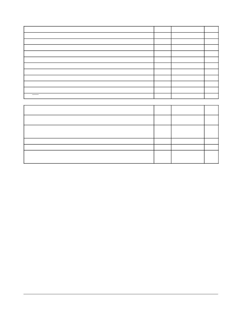
�MAXIMUM� RATINGS� (measured� vs.� Pin� 4,� unless� otherwise� noted)�
�Rating�
�VCC� Pin� 6�
�Comparator� Inverting� Input� Pin� 5�
�Darlington� Switch� Collector� Pin� 1�
�Darlington� Switch� Emitter� Pin� 2� (Transistor� OFF)�
�Darlington� Switch� Collector� to� Emitter� Pins� 1� ?� 2�
�Darlington� Switch� Current�
�I� pk� Sense� Pin� 7�
�Timing� Capacitor� Pin� Voltage� (Pin� 3)�
�Moisture� Sensitivity� Level�
�Lead� Temperature� Soldering�
�ON/OFF� Pin� voltage�
�Symbol�
�V� CC�
�V� CII�
�V� SWC�
�V� SWE�
�V� SWCE�
�I� SW�
�V� IPK�
�V� TC�
�MSL�
�T� SLD�
�V� ON/OFF�
�Value�
�0� to� +42�
�?� 0.3� to� +� V� CC�
�?� 0.3� to� +� 42�
�?� 0.6� to� +� V� CC�
�?� 0.3� to� +� 42�
�1.5�
�?� 0.3� to� V� CC� +� 0.3�
�?� 0.2� to� +1.4�
�1�
�260�
�(� ?� 0.3� to� +25)� <� V� CC�
�Unit�
�V�
�V�
�V�
�V�
�V�
�A�
�V�
�V�
�?�
�°� C�
�V�
�POWER� DISSIPATION� AND� THERMAL� CHARACTERISTICS�
�PDIP� ?� 8� (Note� 5)�
�Thermal� Resistance� Junction� ?� to� ?� Air�
�SOIC� ?� 8� (Note� 5)�
�Thermal� Resistance� Junction� ?� to� ?� Air�
�DFN� ?� 8� (Note� 5)�
�Thermal� Resistance� Junction� ?� to� ?� Air�
�Thermal� Resistance� Junction� ?� to� ?� Case�
�Storage� Temperature� Range�
�Maximum� Junction� Temperature�
�Operating� Junction� Temperature� Range� (Note� 3)�
�NCP3066�
�NCV3066�
�R� q� JA�
�R� q� JA�
�R� q� JA�
�R� q� JC�
�T� STG�
�T� JMAX�
�T� J�
�100�
�180�
�78�
�14�
�?� 65� to� +150�
�+150�
�0� to� +85�
�?� 40� to� +125�
�°� C/W�
�°� C/W�
�°� C/W�
�°� C�
�°� C�
�°� C�
�Stresses� exceeding� Maximum� Ratings� may� damage� the� device.� Maximum� Ratings� are� stress� ratings� only.� Functional� operation� above� the�
�Recommended� Operating� Conditions� is� not� implied.� Extended� exposure� to� stresses� above� the� Recommended� Operating� Conditions� may� affect�
�device� reliability.�
�1.� This� device� series� contains� ESD� protection� and� exceeds� the� following� tests:�
�Pin� 1� ?� 8:� Human� Body� Model� 2000� V� per� AEC� Q100� ?� 002;� 003� or� JESD22/A114;� A115�
�Machine� Model� Method� 200� V�
�2.� This� device� contains� latch� ?� up� protection� and� exceeds� 100� mA� per� JEDEC� Standard� JESD78.�
�3.� The� relation� between� junction� temperature,� ambient� temperature� and� Total� Power� dissipated� in� IC� is� T� J� =� T� A� +� R� q� ?� P� D� .�
�4.� The� pins� which� are� not� defined� may� not� be� loaded� by� external� signals.�
�5.� 35� m� m� copper,� 10� cm� 2� copper� area.�
�http://onsemi.com�
�3�
�相关PDF资料 |
PDF描述 |
|---|---|
| NCP5005GEVB | EVAL BOARD FOR NCP5005G |
| NCP5006EVB | EVAL BOARD FOR NCP5006 |
| NCP5030MTTXGEVB | EVAL BOARD FOR NCP5030MTTXG |
| NCP5602EVB | EVAL BOARD FOR NCP5602 |
| NCP5603GEVB | EVAL BOARD FOR NCP5603G HI FREQ |
相关代理商/技术参数 |
参数描述 |
|---|---|
| NCP3066SCBSTGEVB | 功能描述:电源管理IC开发工具 NCP3066 SOIC8 BOOST DB RoHS:否 制造商:Maxim Integrated 产品:Evaluation Kits 类型:Battery Management 工具用于评估:MAX17710GB 输入电压: 输出电压:1.8 V |
| NCP308MT090TBG | 功能描述:监控电路 RoHS:否 制造商:STMicroelectronics 监测电压数: 监测电压: 欠电压阈值: 过电压阈值: 输出类型:Active Low, Open Drain 人工复位:Resettable 监视器:No Watchdog 电池备用开关:No Backup 上电复位延迟(典型值):10 s 电源电压-最大:5.5 V 最大工作温度:+ 85 C 安装风格:SMD/SMT 封装 / 箱体:UDFN-6 封装:Reel |
| NCP308MT120TBG | 功能描述:监控电路 RoHS:否 制造商:STMicroelectronics 监测电压数: 监测电压: 欠电压阈值: 过电压阈值: 输出类型:Active Low, Open Drain 人工复位:Resettable 监视器:No Watchdog 电池备用开关:No Backup 上电复位延迟(典型值):10 s 电源电压-最大:5.5 V 最大工作温度:+ 85 C 安装风格:SMD/SMT 封装 / 箱体:UDFN-6 封装:Reel |
| NCP308MT125TBG | 功能描述:监控电路 RoHS:否 制造商:STMicroelectronics 监测电压数: 监测电压: 欠电压阈值: 过电压阈值: 输出类型:Active Low, Open Drain 人工复位:Resettable 监视器:No Watchdog 电池备用开关:No Backup 上电复位延迟(典型值):10 s 电源电压-最大:5.5 V 最大工作温度:+ 85 C 安装风格:SMD/SMT 封装 / 箱体:UDFN-6 封装:Reel |
| NCP308MT150TBG | 功能描述:监控电路 RoHS:否 制造商:STMicroelectronics 监测电压数: 监测电压: 欠电压阈值: 过电压阈值: 输出类型:Active Low, Open Drain 人工复位:Resettable 监视器:No Watchdog 电池备用开关:No Backup 上电复位延迟(典型值):10 s 电源电压-最大:5.5 V 最大工作温度:+ 85 C 安装风格:SMD/SMT 封装 / 箱体:UDFN-6 封装:Reel |
发布紧急采购,3分钟左右您将得到回复。