- 您现在的位置:买卖IC网 > Datasheet目录996 > NCP3066SCBCKGEVB (ON Semiconductor)EVAL BOARD FOR NCP3066SCBCKG Datasheet资料下载
参数资料
| 型号: | NCP3066SCBCKGEVB |
| 厂商: | ON Semiconductor |
| 文件页数: | 7/20页 |
| 文件大小: | 0K |
| 描述: | EVAL BOARD FOR NCP3066SCBCKG |
| 设计资源: | NCP3066 Buck SOIC EVB BOM NCP3066SCBCKGEVB Gerber Files NCP3066 BUCK EVB Schematic |
| 标准包装: | 1 |
| 电流 - 输出 / 通道: | 150mA |
| 输出及类型: | 1,非隔离 |
| 输出电压: | 3.2V |
| 特点: | 亮度控制 |
| 输入电压: | 12V |
| 已供物品: | 板 |
| 已用 IC / 零件: | NCP3066 |
| 其它名称: | NCP3066SCBCKGEVBOS |
�� �
�
�NCP3066,� NCV3066�
�INTRODUCTION�
�The� NCP3066� is� a� monolithic� power� switching� regulator�
�optimized� for� LED� Driver� applications.� Its� flexible�
�architecture� enables� the� system� designer� to� directly�
�implement� step� ?� up,� step� ?� down,� and� voltage� ?� inverting�
�converters� with� a� minimum� number� of� external� components�
�for� driving� LEDs.� A� representative� block� diagram� is� shown�
�in� Figure� 3.�
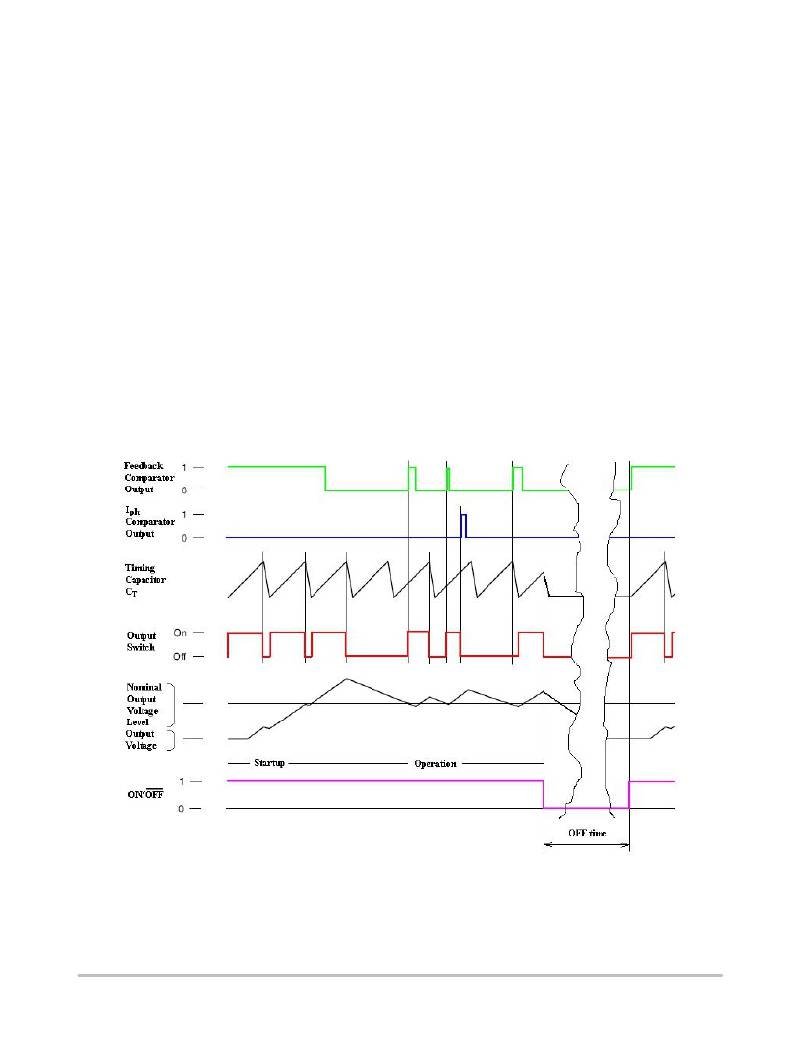
�Operating� Description�
�The� NCP3066� operates� as� a� fixed� oscillator� frequency�
�output� voltage� ripple� gated� regulator.� In� general,� this� mode�
�of� operation� is� somewhat� analogous� to� a� capacitor� charge�
�pump� and� does� not� require� dominant� pole� loop�
�compensation� for� converter� stability.� The� typical� operating�
�waveforms� are� shown� in� Figure� 12.� The� output� voltage�
�waveform� is� shown� for� a� step� ?� down� converter� with� the�
�ripple� and� phasing� exaggerated� for� clarity.� During� initial�
�converter� startup,� the� feedback� comparator� senses� that� the�
�output� voltage� level� is� below� nominal.� This� causes� the�
�output� switch� to� turn� on� and� off� at� a� frequency� and� duty� cycle�
�controlled� by� the� oscillator,� thus� pumping� up� the� output� filter�
�comparator� value,� the� output� switch� cycle� is� inhibited.� When�
�the� load� current� causes� the� output� voltage� to� fall� below� the�
�nominal� value� feedback� comparator� enables� switching�
�immediately.� Under� these� conditions,� the� output� switch�
�conduction� can� be� enabled� for� a� partial� oscillator� cycle,� a�
�partial� cycle� plus� a� complete� cycle,� multiple� cycles,� or� a�
�partial� cycle� plus� multiple� cycles.�
�Oscillator�
�The� oscillator� frequency� and� off� ?� time� of� the� output� switch�
�are� programmed� by� the� value� of� the� timing� capacitor� C� T� .� The�
�capacitor� C� T� is� charged� and� discharged� by� a� 1� to� 6� ratio�
�internal� current� source� and� sink,� generating� a� positive� going�
�sawtooth� waveform� at� Pin� 3.� This� ratio� sets� the� maximum�
�t� ON� /(t� ON� +� t� OFF� )� of� the� switching� converter� as� 6/(6+1)� or�
�85.7%� (typical).� The� oscillator� peak� and� valley� voltage�
�difference� is� 500� mV� typically.� To� calculate� the� C� T� capacitor�
�value� for� required� oscillator� frequency,� use� the� equations�
�found� in� Figure� 15.� An� online� NCP3066� design� tool� can� be�
�found� at� www.onsemi.com,� which� aids� in� selecting�
�component� values.�
�capacitor.� When� the� output� voltage� level� reaches� nominal�
�Figure� 12.� Typical� Operating� Waveforms�
�http://onsemi.com�
�7�
�相关PDF资料 |
PDF描述 |
|---|---|
| NCP5005GEVB | EVAL BOARD FOR NCP5005G |
| NCP5006EVB | EVAL BOARD FOR NCP5006 |
| NCP5030MTTXGEVB | EVAL BOARD FOR NCP5030MTTXG |
| NCP5602EVB | EVAL BOARD FOR NCP5602 |
| NCP5603GEVB | EVAL BOARD FOR NCP5603G HI FREQ |
相关代理商/技术参数 |
参数描述 |
|---|---|
| NCP3066SCBSTGEVB | 功能描述:电源管理IC开发工具 NCP3066 SOIC8 BOOST DB RoHS:否 制造商:Maxim Integrated 产品:Evaluation Kits 类型:Battery Management 工具用于评估:MAX17710GB 输入电压: 输出电压:1.8 V |
| NCP308MT090TBG | 功能描述:监控电路 RoHS:否 制造商:STMicroelectronics 监测电压数: 监测电压: 欠电压阈值: 过电压阈值: 输出类型:Active Low, Open Drain 人工复位:Resettable 监视器:No Watchdog 电池备用开关:No Backup 上电复位延迟(典型值):10 s 电源电压-最大:5.5 V 最大工作温度:+ 85 C 安装风格:SMD/SMT 封装 / 箱体:UDFN-6 封装:Reel |
| NCP308MT120TBG | 功能描述:监控电路 RoHS:否 制造商:STMicroelectronics 监测电压数: 监测电压: 欠电压阈值: 过电压阈值: 输出类型:Active Low, Open Drain 人工复位:Resettable 监视器:No Watchdog 电池备用开关:No Backup 上电复位延迟(典型值):10 s 电源电压-最大:5.5 V 最大工作温度:+ 85 C 安装风格:SMD/SMT 封装 / 箱体:UDFN-6 封装:Reel |
| NCP308MT125TBG | 功能描述:监控电路 RoHS:否 制造商:STMicroelectronics 监测电压数: 监测电压: 欠电压阈值: 过电压阈值: 输出类型:Active Low, Open Drain 人工复位:Resettable 监视器:No Watchdog 电池备用开关:No Backup 上电复位延迟(典型值):10 s 电源电压-最大:5.5 V 最大工作温度:+ 85 C 安装风格:SMD/SMT 封装 / 箱体:UDFN-6 封装:Reel |
| NCP308MT150TBG | 功能描述:监控电路 RoHS:否 制造商:STMicroelectronics 监测电压数: 监测电压: 欠电压阈值: 过电压阈值: 输出类型:Active Low, Open Drain 人工复位:Resettable 监视器:No Watchdog 电池备用开关:No Backup 上电复位延迟(典型值):10 s 电源电压-最大:5.5 V 最大工作温度:+ 85 C 安装风格:SMD/SMT 封装 / 箱体:UDFN-6 封装:Reel |
发布紧急采购,3分钟左右您将得到回复。