- 您现在的位置:买卖IC网 > Datasheet目录996 > NCP3066SCBCKGEVB (ON Semiconductor)EVAL BOARD FOR NCP3066SCBCKG Datasheet资料下载
参数资料
| 型号: | NCP3066SCBCKGEVB |
| 厂商: | ON Semiconductor |
| 文件页数: | 8/20页 |
| 文件大小: | 0K |
| 描述: | EVAL BOARD FOR NCP3066SCBCKG |
| 设计资源: | NCP3066 Buck SOIC EVB BOM NCP3066SCBCKGEVB Gerber Files NCP3066 BUCK EVB Schematic |
| 标准包装: | 1 |
| 电流 - 输出 / 通道: | 150mA |
| 输出及类型: | 1,非隔离 |
| 输出电压: | 3.2V |
| 特点: | 亮度控制 |
| 输入电压: | 12V |
| 已供物品: | 板 |
| 已用 IC / 零件: | NCP3066 |
| 其它名称: | NCP3066SCBCKGEVBOS |
�� �
�
�NCP3066,� NCV3066�
�Peak� Current� Sense� Comparator�
�Under� normal� conditions,� the� output� switch� conduction� is�
�initiated� by� the� Voltage� Feedback� comparator� and�
�terminated� by� the� oscillator.� Abnormal� operating� conditions�
�occur� when� the� converter� output� is� overloaded� or� when�
�feedback� voltage� sensing� is� lost.� Under� these� conditions,� the�
�I� pk� Current� Sense� comparator� will� protect� the� Darlington�
�output� Switch.� The� switch� current� is� converted� to� a� voltage�
�by� inserting� a� fractional� ohm� resistor,� R� Sense� ,� in� series� with�
�V� CC� and� Darlington� output� switch.� The� voltage� drop� across�
�R� Sense� is� monitored� by� the� Current� Sense� comparator.� If� the�
�voltage� drop� exceeds� 200� mV� (nom)� with� respect� to� V� CC� ,� the�
�comparator� will� set� the� latch� and� terminate� the� output� switch�
�conduction� on� a� cycle� ?� by� ?� cycle� basis.�
�Darlington� Switch� is� enabled� again� when� the� chip�
�temperature� decreases� under� the� low� threshold.� This� feature�
�is� provided� to� prevent� catastrophic� failures� from� accidental�
�device� overheating.� It� is� not� intended� to� be� used� as� a�
�replacement� for� proper� heatsinking.�
�Output� Switch�
�The� output� switch� is� designed� in� Darlington�
�configuration.� This� allows� the� application� designer� to�
�operate� at� all� conditions� at� high� switching� speed� and� low�
�voltage� drop.� The� Darlington� Output� Switch� is� designed� to�
�switch� a� maximum� of� 40� V� collector� to� emitter� voltage� and�
�current� up� to� 1.5� A.�
�ON/OFF� Function�
�The� ON/OFF� function� provides� interruption� of� switching�
�Real�
�V� turn� ?� off� on�
�R� s� Resistor�
�V� ipk(sense)�
�di/dt� slope�
�Io�
�t_delay�
�I1�
�I� through� the�
�Darlington�
�Switch�
�and� puts� the� circuitry� into� the� low� consumption� mode.� This�
�feature� is� applicable� for� digital� dimming� of� the� LEDs� as�
�well.� The� ON/OFF� signal� inhibits� switching� of� the� regulator�
�and� reduces� the� average� current� through� the� LEDs.� The�
�frequency� of� this� pulse� width� ?� modulated� signal� with� the�
�duty� cycle� can� range� from� less� than� 1%� to� 100%� is� limited�
�by� the� value� of� 1� kHz.�
�Pulling� this� pin� below� 0.8� V� or� leaving� it� opened� turns� the�
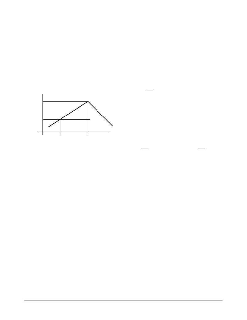
�Figure� 13.� Current� Sense� Waveform�
�The� V� IPK(Sense)� Current� Limit� Sense� Voltage� threshold� is�
�specified� at� static� conditions.� In� dynamic� operation� the�
�sensed� current� turn� ?� off� value� depends� on� comparator�
�response� time� and� di/dt� current� slope.�
�Real� V� turn� ?� off� on� R� sc� resistor�
�V� turn_off� =� V� ipk(sense)� +� R� Sense� *(t� delay� *di/dt)�
�Typical� I� pk� comparator� response� time� t� delay� is� 350� ns.� The�
�di/dt� current� slope� is� dependent� on� the� voltage� difference�
�across� the� inductor� and� the� value� of� the� inductor.� Increasing�
�the� value� of� the� inductor� will� reduce� the� di/dt� slope.�
�It� is� recommended� to� verify� the� actual� peak� current� in� the�
�application� at� worst� conditions� to� be� sure� that� the� max� peak�
�current� will� never� get� over� the� 1.5� A� Darlington� Switch�
�Current� max� rating.�
�Thermal� Shutdown�
�Internal� thermal� shutdown� circuitry� is� provided� to� protect�
�the� IC� in� the� event� that� the� maximum� junction� temperature�
�is� exceeded.� When� activated,� typically� at� 160� °� C,� the�
�Darlington� Output� Switch� is� disabled.� The� temperature�
�sensing� circuit� is� designed� with� some� hysteresis.� The�
�regulator� off.� In� this� state� the� consumption� of� the� device� is�
�reduced� below� 100� uA.� Pulling� this� pin� above� 2.4� V� (up� to�
�max.� 25� V)� allows� the� regulator� running� in� normal� state.� If�
�the� ON/OFF� feature� is� not� needed,� the� ON/OFF� pin� can� be�
�wired� to� V� CC� ,� provided� this� voltage� does� not� exceed� 25� V.�
�No� Output� Capacitor� Operation�
�A� traditional� buck� topology� includes� an� inductor� followed�
�by� an� output� capacitor� which� filters� the� ripple.� The� capacitor�
�is� placed� in� parallel� with� the� LED� or� array� of� LEDs� to� lower�
�the� ripple� current.� A� constant� current� buck� regulator� such� as�
�the� NCP3066� focuses� on� the� control� of� the� current� through�
�the� load,� not� the� voltage� across� it.� The� switching� frequency�
�of� the� NCP3066� is� in� the� range� of� 100� ?� 250� kHz� which� is�
�much� higher� than� the� human� eye� can� detect.� By� configuring�
�the� NCP3066� in� a� continuous� conduction� buck�
�configuration� with� low� peak� to� peak� ripple� the� output� filter�
�capacitor� can� be� eliminated.� The� important� design�
�parameter� is� to� keep� the� peak� current� below� the� maximum�
�current� rating� of� the� LED.� Using� 15� ?� 40%� peak� to� peak� ripple�
�results� in� a� good� compromise� between� achieving� max�
�average� output� current� without� exceeding� the� maximum�
�limit.� This� saves� space� and� reduces� part� count� for�
�applications.�
�http://onsemi.com�
�8�
�相关PDF资料 |
PDF描述 |
|---|---|
| NCP5005GEVB | EVAL BOARD FOR NCP5005G |
| NCP5006EVB | EVAL BOARD FOR NCP5006 |
| NCP5030MTTXGEVB | EVAL BOARD FOR NCP5030MTTXG |
| NCP5602EVB | EVAL BOARD FOR NCP5602 |
| NCP5603GEVB | EVAL BOARD FOR NCP5603G HI FREQ |
相关代理商/技术参数 |
参数描述 |
|---|---|
| NCP3066SCBSTGEVB | 功能描述:电源管理IC开发工具 NCP3066 SOIC8 BOOST DB RoHS:否 制造商:Maxim Integrated 产品:Evaluation Kits 类型:Battery Management 工具用于评估:MAX17710GB 输入电压: 输出电压:1.8 V |
| NCP308MT090TBG | 功能描述:监控电路 RoHS:否 制造商:STMicroelectronics 监测电压数: 监测电压: 欠电压阈值: 过电压阈值: 输出类型:Active Low, Open Drain 人工复位:Resettable 监视器:No Watchdog 电池备用开关:No Backup 上电复位延迟(典型值):10 s 电源电压-最大:5.5 V 最大工作温度:+ 85 C 安装风格:SMD/SMT 封装 / 箱体:UDFN-6 封装:Reel |
| NCP308MT120TBG | 功能描述:监控电路 RoHS:否 制造商:STMicroelectronics 监测电压数: 监测电压: 欠电压阈值: 过电压阈值: 输出类型:Active Low, Open Drain 人工复位:Resettable 监视器:No Watchdog 电池备用开关:No Backup 上电复位延迟(典型值):10 s 电源电压-最大:5.5 V 最大工作温度:+ 85 C 安装风格:SMD/SMT 封装 / 箱体:UDFN-6 封装:Reel |
| NCP308MT125TBG | 功能描述:监控电路 RoHS:否 制造商:STMicroelectronics 监测电压数: 监测电压: 欠电压阈值: 过电压阈值: 输出类型:Active Low, Open Drain 人工复位:Resettable 监视器:No Watchdog 电池备用开关:No Backup 上电复位延迟(典型值):10 s 电源电压-最大:5.5 V 最大工作温度:+ 85 C 安装风格:SMD/SMT 封装 / 箱体:UDFN-6 封装:Reel |
| NCP308MT150TBG | 功能描述:监控电路 RoHS:否 制造商:STMicroelectronics 监测电压数: 监测电压: 欠电压阈值: 过电压阈值: 输出类型:Active Low, Open Drain 人工复位:Resettable 监视器:No Watchdog 电池备用开关:No Backup 上电复位延迟(典型值):10 s 电源电压-最大:5.5 V 最大工作温度:+ 85 C 安装风格:SMD/SMT 封装 / 箱体:UDFN-6 封装:Reel |
发布紧急采购,3分钟左右您将得到回复。