参数资料
| 型号: | NCP5332ADW |
| 厂商: | ON Semiconductor |
| 文件页数: | 14/30页 |
| 文件大小: | 0K |
| 描述: | IC CTLR BUCK 2PH DRVR/DAC 28SOIC |
| 产品变化通告: | Product Obsolescence 30/Sept/2009 |
| 标准包装: | 26 |
| 应用: | 控制器,高性能处理器 |
| 输入电压: | 4.5 V ~ 14 V |
| 输出数: | 2 |
| 输出电压: | 可调 |
| 工作温度: | 0°C ~ 70°C |
| 安装类型: | 表面贴装 |
| 封装/外壳: | 28-SOIC(0.295",7.50mm 宽) |
| 供应商设备封装: | 28-SOIC |
| 包装: | 管件 |
第1页第2页第3页第4页第5页第6页第7页第8页第9页第10页第11页第12页第13页当前第14页第15页第16页第17页第18页第19页第20页第21页第22页第23页第24页第25页第26页第27页第28页第29页第30页
�� �
�
�NCP5332A�
�SWNODE�
�R� CSn�
�n� =� 1� or� 2�
�Ln�
�CSn�
�+�
�CSA�
�COn�
�C� CSn�
�RLn�
�Internal� Ramp�
�V� OUT�
�(V� CORE� )�
�+�
�CS� REF�
�“Fast?Feedback”�
�Connection�
�?+�
�Channel�
�Start?Up�
�+�
�To� F/F�
�Reset�
�V� FB�
�DAC�
�Out�
�E.A.�
�+�
�Offset�
�PWM�
�COMP�
�COMP�
�+�
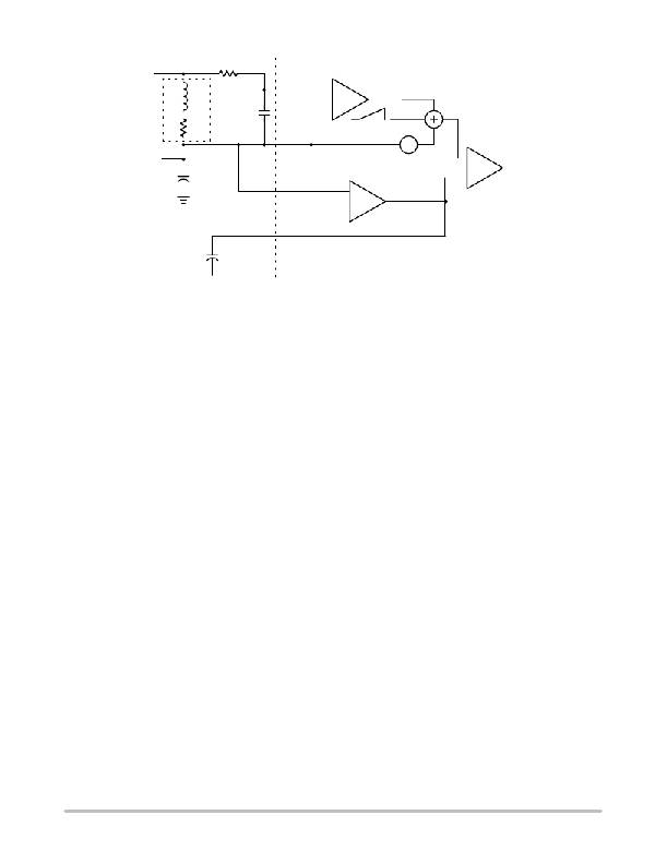
�Figure� 12.� Enhanced� V� 2� Control� Employing� Lossless� Inductive� Current� Sensing� and� Internal� Ramp�
�Inductive� Current� Sensing�
�For� lossless� sensing,� current� can� be� sensed� across� the�
�inductor� as� shown� in� Figure� 12.� In� the� diagram,� L� is� the�
�output� inductance� and� R� L� is� the� inherent� inductor� resistance.�
�To� compensate� the� current� sense� signal,� the� values� of� R� CSn�
�and� C� CSn� are� chosen� so� that� L/R� L� =� R� CSn� ?� C� CSn� .� If� this�
�criteria� is� met,� the� current� sense� signal� will� be� the� same� shape�
�as� the� inductor� current� and� the� voltage� signal� at� CSn� will�
�represent� the� instantaneous� value� of� inductor� current.� Also,�
�the� circuit� can� be� analyzed� as� if� a� sense� resistor� of� value� R� L�
�was� used� as� a� sense� resistor� (R� S� ).�
�When� choosing� or� designing� inductors� for� use� with�
�inductive� sensing,� tolerances� and� temperature� effects� should�
�be� considered.� Cores� with� a� low� permeability� material� or� a�
�large� gap� will� usually� have� minimal� inductance� change� with�
�temperature� and� load.� Copper� magnet� wire� has� a�
�temperature� coefficient� of� 0.39%� per� °� C.� The� increase� in�
�winding� resistance� at� higher� temperatures� should� be�
�considered� when� setting� the� I� LIM� threshold.� If� a� more�
�accurate� current� sense� is� required� than� inductive� sensing� can�
�provide,� current� can� be� sensed� through� a� resistor� as� shown�
�in� Figure� 10.�
�Current� Sharing� Accuracy�
�Printed� circuit� board� (PCB)� traces� that� carry� inductor�
�current� can� be� used� as� part� of� the� current� sense� resistance�
�depending� on� where� the� current� sense� signal� is� picked� off.�
�For� accurate� current� sharing,� the� current� sense� inputs� should�
�sense� the� current� at� relatively� the� same� point� for� each� phase�
�and� the� connection� to� the� CS� REF� pin� should� be� made� so� that�
�no� phase� is� favored.� In� some� cases,� especially� with� inductive�
�sensing,� resistance� of� the� PCB� can� be� useful� for� increasing�
�the� current� sense� resistance.� The� total� current� sense�
�resistance� used� for� calculations� must� include� any� PCB� trace�
�resistance� between� the� CSn� input� and� the� CS� REF� input� that�
�carries� inductor� current.�
�Current� Sense� Amplifier� (CSA)� input� mismatch� and� the�
�value� of� the� current� sense� component� will� determine� the�
�accuracy� of� the� current� sharing� between� phases.� The� worst�
�case� Current� Sense� Amplifier� input� mismatch� is� ±� 5.0� mV�
�and� will� typically� be� within� 3.0� mV.� The� difference� in� peak�
�currents� between� phases� will� be� the� CSA� input� mismatch�
�divided� by� the� current� sense� resistance.� If� all� current� sense�
�components� are� of� equal� resistance� a� 3.0� mV� mismatch� with�
�a� 2.0� m� ?� sense� resistance� will� produce� a� 1.5� A� difference� in�
�current� between� phases.�
�External� Ramp� Size� and� Current� Sensing�
�The� internal� ramp� allows� flexibility� of� current� sense� time�
�constant.� Typically,� the� current� sense� R� CSn� ?� C� CSn� time�
�constant� (n� =� 1� or� 2)� should� be� equal� to� or� slower� than� the�
�inductor� ’s� time� constant.� If� RC� is� chosen� to� be� smaller�
�(faster)� than� L/R� L� ,� the� AC� or� transient� portion� of� the� current�
�sensing� signal� will� be� scaled� larger� than� the� DC� portion.� This�
�will� provide� a� larger� steady� state� ramp,� but� circuit�
�performance� will� be� affected� and� must� be� evaluated�
�carefully.� The� current� signal� will� overshoot� during� transients�
�and� settle� at� the� rate� determined� by� R� CSn� ?� C� CSn� .� It� will�
�eventually� settle� to� the� correct� DC� level,� but� the� error� will�
�decay� with� the� time� constant� of� R� CSn� ?� C� CSn� .� If� this� error� is�
�excessive� it� will� effect� transient� response,� adaptive�
�positioning� and� current� limit.� During� a� positive� current�
�transient,� the� COMP� pin� will� be� required� to� undershoot� in�
�response� to� the� current� signal� in� order� to� maintain� the� output�
�voltage.� Similarly,� the� V� DRP� signal� will� overshoot� which�
�will� produce� too� much� transient� droop� in� the� output� voltage.�
�Single� phase� overcurrent� will� trip� earlier� than� it� would� if�
�compensated� correctly� and� hiccup� mode� current� limit� will�
�have� a� lower� threshold� for� fast� rise� step� loads� than� for� slowly�
�rising� output� currents.�
�The� waveforms� in� Figure� 13� show� a� simulation� of� the�
�current� sense� signal� and� the� actual� inductor� current� during� a�
�http://onsemi.com�
�14�
�相关PDF资料 |
PDF描述 |
|---|---|
| NCP5378MNR2G | IC CTLR 1PH SYNC BUCK 32QFN |
| NCP5380AMNR2G | IC CTLR SYNC BUCK SGL 32QFN |
| NCP5381AMNR2G | IC BUCK CTLR 2/3/4PHASE 40-QFN |
| NCP5381MNR2G | IC CTLR BUCK 2/3/4PHASE 40-QFN |
| NCP5382MNR2G | IC BUCK CTLR 2-6PHASE 48-QFN |
相关代理商/技术参数 |
参数描述 |
|---|---|
| NCP5332ADWR2 | 功能描述:DC/DC 开关控制器 2 Phase Buck w/Gate RoHS:否 制造商:Texas Instruments 输入电压:6 V to 100 V 开关频率: 输出电压:1.215 V to 80 V 输出电流:3.5 A 输出端数量:1 最大工作温度:+ 125 C 安装风格: 封装 / 箱体:CPAK |
| NCP5338MNR2G | 制造商:ON Semiconductor 功能描述:INTEGRATED DRIVER AND MOS - Tape and Reel 制造商:ON Semiconductor 功能描述:INTEGRATED DRIVER AND MOS - Cut TR (SOS) 制造商:ON Semiconductor 功能描述:REEL / INTEGRATED DRIVER AND MOS 制造商:ON Semiconductor 功能描述:Integrated Driver and MOSFET |
| NCP5351 | 制造商:ONSEMI 制造商全称:ON Semiconductor 功能描述:4 A Synchronous Buck Power MOSFET Driver |
| NCP5351/D | 制造商:未知厂家 制造商全称:未知厂家 功能描述:4A Synchronous Buck Power Mosfet Driver |
| NCP5351D | 功能描述:功率驱动器IC 5V 4A Dual MOSFET RoHS:否 制造商:Micrel 产品:MOSFET Gate Drivers 类型:Low Cost High or Low Side MOSFET Driver 上升时间: 下降时间: 电源电压-最大:30 V 电源电压-最小:2.75 V 电源电流: 最大功率耗散: 最大工作温度:+ 85 C 安装风格:SMD/SMT 封装 / 箱体:SOIC-8 封装:Tube |
发布紧急采购,3分钟左右您将得到回复。