参数资料
| 型号: | NCP5332ADW |
| 厂商: | ON Semiconductor |
| 文件页数: | 15/30页 |
| 文件大小: | 0K |
| 描述: | IC CTLR BUCK 2PH DRVR/DAC 28SOIC |
| 产品变化通告: | Product Obsolescence 30/Sept/2009 |
| 标准包装: | 26 |
| 应用: | 控制器,高性能处理器 |
| 输入电压: | 4.5 V ~ 14 V |
| 输出数: | 2 |
| 输出电压: | 可调 |
| 工作温度: | 0°C ~ 70°C |
| 安装类型: | 表面贴装 |
| 封装/外壳: | 28-SOIC(0.295",7.50mm 宽) |
| 供应商设备封装: | 28-SOIC |
| 包装: | 管件 |
第1页第2页第3页第4页第5页第6页第7页第8页第9页第10页第11页第12页第13页第14页当前第15页第16页第17页第18页第19页第20页第21页第22页第23页第24页第25页第26页第27页第28页第29页第30页
�� �
�
�NCP5332A�
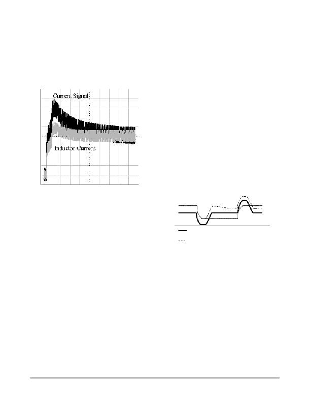
�positive� step� in� load� current� with� values� of� L� =� 500� nH,� R� L�
�=� 1.6� m� ?� ,� R� CSn� =� 20� k� and� C� CSn� =� 0.01� μ� F.� For� ideal� current�
�signal� compensation� the� value� of� R� CSn� should� be� 31� k� ?� .� Due�
�to� the� faster� than� ideal� RC� time� constant� there� is� an� overshoot�
�of� 50%� and� the� overshoot� decays� with� a� 200� μ� s� time�
�constant.� With� this� compensation� the� I� LIM� pin� threshold�
�must� be� set� more� than� 50%� above� the� full� load� current� to�
�avoid� triggering� hiccup� mode� during� a� large� output� load�
�step.�
�Transient� Response� and� Adaptive� Positioning�
�For� applications� with� fast� transient� currents� the� output� filter�
�is� frequently� sized� larger� than� ripple� currents� require� in� order�
�to� reduce� voltage� excursions� during� load� transients.� Adaptive�
�voltage� positioning� can� reduce� peak?to?peak� output� voltage�
�deviations� during� load� transients� and� allow� for� a� smaller�
�output� filter.� The� output� voltage� can� be� set� higher� than�
�nominal� at� light� loads� to� reduce� output� voltage� sag� when� the�
�load� current� is� applied.� Similarly,� the� output� voltage� can� be� set�
�lower� than� nominal� during� heavy� loads� to� reduce� overshoot�
�when� the� load� current� is� removed.� For� low� current�
�applications� a� droop� resistor� can� provide� fast� accurate� adaptive�
�positioning.� However,� at� high� currents� the� loss� in� a� droop�
�resistor� becomes� excessive.� For� example;� in� a� 50� A� converter�
�a� 1� m� ?� resistor� to� provide� a� 50� mV� change� in� output� voltage�
�between� no� load� and� full� load� would� dissipate� 2.5� Watts.�
�Lossless� adaptive� positioning� is� an� alternative� to� using� a�
�droop� resistor,� but� must� respond� to� changes� in� load� current.�
�Figure� 14� shows� how� adaptive� positioning� works.� The�
�waveform� labeled� normal� shows� a� converter� without�
�adaptive� positioning.� On� the� left,� the� output� voltage� sags�
�when� the� output� current� is� stepped� up� and� later� overshoots�
�when� current� is� stepped� back� down.� With� fast� (ideal)�
�adaptive� positioning� the� peak� to� peak� excursions� are� cut� in�
�half.� In� the� slow� adaptive� positioning� waveform� the� output�
�voltage� is� not� repositioned� quickly� enough� after� current� is�
�stepped� up� and� the� upper� limit� is� exceeded.�
�Figure� 13.� Inductive� Sensing� Waveform� During� a�
�Load� Step� with� Fast� RC� Time� Constant� (50� μ� s/div)�
�Current� Limit�
�Two� levels� of� overcurrent� protection� are� provided.� First,�
�if� the� voltage� on� the� Current� Sense� pins� (either� CS1� or� CS2)�
�exceeds� CS� REF� by� more� than� a� fixed� threshold� (Single� Pulse�
�Current� Limit),� the� PWM� comparator� is� turned� off.� This�
�provides� fast� peak� current� protection� for� individual� phases.�
�Second,� the� individual� phase� currents� are� summed� and�
�low?pass� filtered� to� compare� an� averaged� current� signal� to�
�a� user� adjustable� voltage� on� the� I� LIM� pin.� If� the� I� LIM� voltage�
�is� exceeded,� the� fault� latch� trips� and� the� Soft� Start� capacitor�
�is� discharged� until� the� Soft?Start� pin� reaches� 0.27� V.� Then�
�Soft� Start� begins.� The� converter� will� continue� to� operate� in�
�a� low� current� hiccup� mode� until� the� fault� condition� is�
�corrected.�
�Overvoltage� Protection�
�Overvoltage� protection� (OVP)� is� provided� as� a� result� of�
�the� normal� operation� of� the� Enhanced� V� 2� control� topology�
�with� synchronous� rectifiers.� The� control� loop� responds� to� an�
�overvoltage� condition� within� 400� ns,� causing� the� top�
�MOSFET� to� shut� OFF� and� the� synchronous� (lower)�
�MOSFET� to� turn� ON.� This� results� in� a� “crowbar”� action� to�
�clamp� the� output� voltage� and� prevent� damage� to� the� load.�
�The� regulator� will� remain� in� this� state� until� the� overvoltage�
�condition� ceases� or� the� input� voltage� is� pulled� low.�
�Normal�
�Fast� Adaptive� Positioning�
�Slow� Adaptive� Positioning�
�Limits�
�Figure� 14.� Adaptive� Positioning�
�The� controller� can� be� configured� to� adjust� the� output�
�voltage� based� on� the� output� current� of� the� converter.� (Refer�
�to� the� application� diagram� in� Figure� 1).� To� set� the� no?load�
�positioning,� a� resistor� is� placed� between� the� output� voltage�
�and� V� FB� pin.� The� V� FB� bias� current� will� develop� a� voltage�
�across� the� resistor� to� adjust� the� no?load� output� voltage.� The�
�V� FB� bias� current� is� dependent� on� the� value� of� R� OSC� as� shown�
�in� the� datasheet.�
�During� no� load� conditions� the� V� DRP� pin� is� at� the� same�
�voltage� as� the� V� FB� pin,� so� none� of� the� V� FB� bias� current� flows�
�through� the� V� DRP� resistor.� When� output� current� increases�
�the� V� DRP� pin� increases� proportionally� and� the� V� DRP� pin�
�current� offsets� the� V� FB� bias� current� and� causes� the� output�
�voltage� to� decrease.�
�The� response� during� the� first� few� microseconds� of� a� load�
�transient� are� controlled� primarily� by� power� stage� output�
�impedance� and� the� ESR� and� ESL� of� the� output� filter.� The�
�http://onsemi.com�
�15�
�相关PDF资料 |
PDF描述 |
|---|---|
| NCP5378MNR2G | IC CTLR 1PH SYNC BUCK 32QFN |
| NCP5380AMNR2G | IC CTLR SYNC BUCK SGL 32QFN |
| NCP5381AMNR2G | IC BUCK CTLR 2/3/4PHASE 40-QFN |
| NCP5381MNR2G | IC CTLR BUCK 2/3/4PHASE 40-QFN |
| NCP5382MNR2G | IC BUCK CTLR 2-6PHASE 48-QFN |
相关代理商/技术参数 |
参数描述 |
|---|---|
| NCP5332ADWR2 | 功能描述:DC/DC 开关控制器 2 Phase Buck w/Gate RoHS:否 制造商:Texas Instruments 输入电压:6 V to 100 V 开关频率: 输出电压:1.215 V to 80 V 输出电流:3.5 A 输出端数量:1 最大工作温度:+ 125 C 安装风格: 封装 / 箱体:CPAK |
| NCP5338MNR2G | 制造商:ON Semiconductor 功能描述:INTEGRATED DRIVER AND MOS - Tape and Reel 制造商:ON Semiconductor 功能描述:INTEGRATED DRIVER AND MOS - Cut TR (SOS) 制造商:ON Semiconductor 功能描述:REEL / INTEGRATED DRIVER AND MOS 制造商:ON Semiconductor 功能描述:Integrated Driver and MOSFET |
| NCP5351 | 制造商:ONSEMI 制造商全称:ON Semiconductor 功能描述:4 A Synchronous Buck Power MOSFET Driver |
| NCP5351/D | 制造商:未知厂家 制造商全称:未知厂家 功能描述:4A Synchronous Buck Power Mosfet Driver |
| NCP5351D | 功能描述:功率驱动器IC 5V 4A Dual MOSFET RoHS:否 制造商:Micrel 产品:MOSFET Gate Drivers 类型:Low Cost High or Low Side MOSFET Driver 上升时间: 下降时间: 电源电压-最大:30 V 电源电压-最小:2.75 V 电源电流: 最大功率耗散: 最大工作温度:+ 85 C 安装风格:SMD/SMT 封装 / 箱体:SOIC-8 封装:Tube |
发布紧急采购,3分钟左右您将得到回复。