参数资料
| 型号: | NCP5332ADW |
| 厂商: | ON Semiconductor |
| 文件页数: | 18/30页 |
| 文件大小: | 0K |
| 描述: | IC CTLR BUCK 2PH DRVR/DAC 28SOIC |
| 产品变化通告: | Product Obsolescence 30/Sept/2009 |
| 标准包装: | 26 |
| 应用: | 控制器,高性能处理器 |
| 输入电压: | 4.5 V ~ 14 V |
| 输出数: | 2 |
| 输出电压: | 可调 |
| 工作温度: | 0°C ~ 70°C |
| 安装类型: | 表面贴装 |
| 封装/外壳: | 28-SOIC(0.295",7.50mm 宽) |
| 供应商设备封装: | 28-SOIC |
| 包装: | 管件 |
第1页第2页第3页第4页第5页第6页第7页第8页第9页第10页第11页第12页第13页第14页第15页第16页第17页当前第18页第19页第20页第21页第22页第23页第24页第25页第26页第27页第28页第29页第30页
�� �
�
�NCP5332A�
�transient� performance� of� the� converter.� When� selecting� an�
�inductor� the� designer� must� consider� factors� such� as� DC�
�current,� peak� current,� output� voltage� ripple,� core� material,�
�magnetic� saturation,� temperature,� physical� size,� and� cost�
�(usually� the� primary� concern).�
�In� general,� the� output� inductance� value� should� be� as� low�
�and� physically� small� as� possible� to� provide� the� best� transient�
�difficult� for� the� converter� to� stay� within� the� regulation� limits�
�when� the� load� is� removed� than� when� it� is� applied� ?� excessive�
�overshoot� may� result.�
�The� output� voltage� ripple� can� be� calculated� using� the�
�output� inductor� value� derived� in� this� Section� (Lo� MIN� ),� the�
�number� of� output� capacitors� (N� OUT,MIN� )� and� the� per�
�capacitor� ESR� determined� in� the� previous� Section:�
�response� and� minimum� cost.� If� a� large� inductance� value� is�
�used,� the� converter� will� not� respond� quickly� to� rapid� changes�
�in� the� load� current.� On� the� other� hand,� too� low� an� inductance�
�VOUT,P?P� +� (ESR� per� cap� NOUT,MIN)� @�
�(VIN� *� #Phases� @� VOUT)� @� D� (LoMIN� @� fSW)�
�(4)�
�value� will� result� in� very� large� ripple� currents� in� the� power�
�components� (MOSFETs,� capacitors,� etc)� resulting� in�
�increased� dissipation� and� lower� converter� efficiency.� Also,�
�increased� ripple� currents� will� force� the� designer� to� use�
�higher� rated� MOSFETs,� oversize� the� thermal� solution,� and�
�use� more,� higher� rated� input� and� output� capacitors� ?� the�
�converter� cost� will� be� adversely� effected.�
�One� method� of� calculating� an� output� inductor� value� is� to�
�size� the� inductor� to� produce� a� specified� maximum� ripple�
�current� in� the� inductor.� Lower� ripple� currents� will� result� in�
�less� core� and� MOSFET� losses� and� higher� converter�
�efficiency.� Equation� 3� may� be� used� to� calculate� the� minimum�
�inductor� value� to� produce� a� given� maximum� ripple� current�
�(� α� )� per� phase.� The� inductor� value� calculated� by� this� equation�
�is� a� minimum� because� values� less� than� this� will� produce� more�
�ripple� current� than� desired.� Conversely,� higher� inductor�
�values� will� result� in� less� than� the� maximum� ripple� current.�
�This� formula� assumes� steady?state� conditions� with� no�
�more� than� one� phase� on� at� any� time.� The� second� term� in�
�Equation� 4� is� the� total� ripple� current� seen� by� the� output�
�capacitors.� The� total� output� ripple� current� is� the� “time�
�summation”� of� the� two� individual� phase� currents� that� are�
�180� degrees� out?of?phase.� As� the� inductor� current� in� one�
�phase� ramps� upward,� current� in� the� other� phase� ramps�
�downward� and� provides� a� canceling� of� currents� during� part�
�of� the� switching� cycle.� Therefore,� the� total� output� ripple�
�current� and� voltage� are� reduced� in� a� multi?phase� converter.�
�3.� Input� Capacitor� Selection�
�The� choice� and� number� of� input� capacitors� is� primarily�
�determined� by� their� voltage� and� ripple� current� ratings.� The�
�designer� must� choose� capacitors� that� will� support� the� worst�
�case� input� voltage� with� adequate� margin.� To� calculate� the�
�number� of� input� capacitors� one� must� first� determine� the� total�
�LoMIN� +�
�(VIN� *� VOUT)� @� VOUT�
�(� a� @� IO,MAX� @� VIN� @� fSW)�
�(3)�
�RMS� input� ripple� current.� To� this� end,� begin� by� calculating�
�the� average� input� current� to� the� converter:�
�IIN,AVG� +� IO,MAX� @� D� h�
�α� is� the� ripple� current� as� a� percentage� of� the� maximum�
�output� current� per� phase� (� α� =� 0.15� for� ±� 15%,� α� =� 0.25� for�
�±� 25%,� etc).� If� the� minimum� inductor� value� is� used,� the�
�inductor� current� will� swing� ±� α� %� about� its� value� at� the� center�
�(1/2� the� DC� output� current� for� a� two?phase� converter).�
�Therefore,� for� a� two?phase� converter,� the� inductor� must� be�
�designed� or� selected� such� that� it� will� not� saturate� with� a� peak�
�current� of� (1� +� α� )� ?� I� O,MAX� /2.�
�The� maximum� inductor� value� is� limited� by� the� transient�
�(5)�
�where:�
�D� is� the� duty� cycle� of� the� converter,� D� =� V� OUT� /V� IN� .�
�η� is� the� specified� minimum� efficiency.�
�I� O,MAX� is� the� maximum� converter� output� current.�
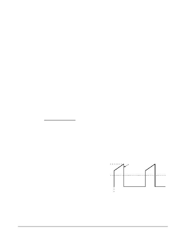
�The� input� capacitors� will� discharge� when� the� control� FET�
�is� ON� and� charge� when� the� control� FET� is� OFF� as� shown� in�
�Figure� 15.�
�response� of� the� converter.� If� the� converter� is� to� have� a� fast�
�transient� response� then� the� inductor� should� be� made� as� small�
�I� C,MAX�
�?� I� C,IN� =� I� C,MAX� ?� I� C,MIN�
�as� possible.� If� the� inductor� is� too� large� its� current� will� change�
�too� slowly,� the� output� voltage� will� droop� excessively,� more�
�bulk� capacitors� will� be� required,� and� the� converter� cost� will�
�I� C,MIN�
�0A�
�t� ON�
�T/2�
�be� increased.� For� a� given� inductor� value,� its� interesting� to�
�determine� the� times� required� to� increase� or� decrease� the�
�current.�
�For� increasing� current:�
�?I� IN,AVG�
�FET� Off,�
�Caps� Charging�
�D� tINC� +� Lo� @� D� IO� (VIN� *� VOUT)�
�For� decreasing� current:�
�D� tDEC� +� Lo� @� D� IO� (VOUT)�
�(3.1)�
�(3.2)�
�FET� On,�
�Caps� Discharging�
�Figure� 15.� Input� Capacitor� Current� for� a�
�Two?Phase� Converter�
�For� typical� processor� applications� with� output� voltages�
�less� than� half� the� input� voltage,� the� current� will� be� increased�
�The� following� equations� will� determine� the� maximum� and�
�minimum� currents� delivered� by� the� input� capacitors:�
�much� more� quickly� than� it� can� be� decreased.� It� may� be� more�
�http://onsemi.com�
�18�
�相关PDF资料 |
PDF描述 |
|---|---|
| NCP5378MNR2G | IC CTLR 1PH SYNC BUCK 32QFN |
| NCP5380AMNR2G | IC CTLR SYNC BUCK SGL 32QFN |
| NCP5381AMNR2G | IC BUCK CTLR 2/3/4PHASE 40-QFN |
| NCP5381MNR2G | IC CTLR BUCK 2/3/4PHASE 40-QFN |
| NCP5382MNR2G | IC BUCK CTLR 2-6PHASE 48-QFN |
相关代理商/技术参数 |
参数描述 |
|---|---|
| NCP5332ADWR2 | 功能描述:DC/DC 开关控制器 2 Phase Buck w/Gate RoHS:否 制造商:Texas Instruments 输入电压:6 V to 100 V 开关频率: 输出电压:1.215 V to 80 V 输出电流:3.5 A 输出端数量:1 最大工作温度:+ 125 C 安装风格: 封装 / 箱体:CPAK |
| NCP5338MNR2G | 制造商:ON Semiconductor 功能描述:INTEGRATED DRIVER AND MOS - Tape and Reel 制造商:ON Semiconductor 功能描述:INTEGRATED DRIVER AND MOS - Cut TR (SOS) 制造商:ON Semiconductor 功能描述:REEL / INTEGRATED DRIVER AND MOS 制造商:ON Semiconductor 功能描述:Integrated Driver and MOSFET |
| NCP5351 | 制造商:ONSEMI 制造商全称:ON Semiconductor 功能描述:4 A Synchronous Buck Power MOSFET Driver |
| NCP5351/D | 制造商:未知厂家 制造商全称:未知厂家 功能描述:4A Synchronous Buck Power Mosfet Driver |
| NCP5351D | 功能描述:功率驱动器IC 5V 4A Dual MOSFET RoHS:否 制造商:Micrel 产品:MOSFET Gate Drivers 类型:Low Cost High or Low Side MOSFET Driver 上升时间: 下降时间: 电源电压-最大:30 V 电源电压-最小:2.75 V 电源电流: 最大功率耗散: 最大工作温度:+ 85 C 安装风格:SMD/SMT 封装 / 箱体:SOIC-8 封装:Tube |
发布紧急采购,3分钟左右您将得到回复。