参数资料
| 型号: | NCP5425DB |
| 厂商: | ON Semiconductor |
| 文件页数: | 13/22页 |
| 文件大小: | 0K |
| 描述: | IC REG CTRLR BUCK PWM VM 20TSSOP |
| 产品变化通告: | Product Obsolescence 14/Apr/2010 |
| 标准包装: | 75 |
| PWM 型: | 电压模式 |
| 输出数: | 2 |
| 频率 - 最大: | 938kHz |
| 占空比: | 100% |
| 电源电压: | 4.75 V ~ 13.2 V |
| 降压: | 是 |
| 升压: | 无 |
| 回扫: | 无 |
| 反相: | 无 |
| 倍增器: | 无 |
| 除法器: | 无 |
| Cuk: | 无 |
| 隔离: | 无 |
| 工作温度: | 0°C ~ 125°C |
| 封装/外壳: | 20-TSSOP(0.173",4.40mm 宽) |
| 包装: | 管件 |
�� �
�
�NCP5425�
�VIN� )� VLFET� +� VHFET� +� VL�
�DESIGN� GUIDELINES�
�General�
�The� output� voltage� tolerance� can� be� affected� by� any� or� all�
�of� the� following:�
�1.� Buck� regulator� output� voltage� set� point� accuracy.�
�2.� Output� voltage� change� due� to� discharging� or�
�charging� of� the� bulk� decoupling� capacitors� during�
�a� load� current� transient.�
�3.� Output� voltage� change� due� to� the� ESR� and� ESL� of�
�the� bulk� and� high� frequency� decoupling� capacitors,�
�circuit� traces,� and� vias.�
�4.� Output� voltage� ripple� and� noise.�
�Budgeting� the� tolerance� is� left� to� the� designer� who� must�
�consider� all� of� the� above� effects� and� provide� an� output�
�voltage� that� will� meet� the� specified� tolerance� at� the� load.� The�
�designer� must� also� ensure� that� the� regulator� component�
�temperatures� are� kept� within� the� manufacturer� ’s� specified�
�ratings� at� full� load� and� maximum� ambient� temperature.�
�Selecting� Feedback� Divider� Resistors�
�V� OUT�
�R1�
�V� FB�
�R2�
�Calculating� Duty� Cycle�
�The� duty� cycle� of� a� buck� converter� (including� parasitic�
�losses)� is� given� by� the� formula:�
�VOUT� )� (VHFET� )� VL)�
�Duty� Cycle� +� D� +�
�where:�
�V� OUT� =� buck� regulator� output� voltage;�
�V� HFET� =� high� side� FET� voltage� drop� due� to� RDS(ON);�
�V� L� =� output� inductor� voltage� drop� due� to� inductor� wire�
�DC� resistance;�
�V� IN� =� buck� regulator� input� voltage;�
�V� LFET� =� low� side� FET� voltage� drop� due� to� RDS(ON).�
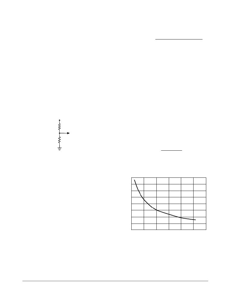
�Switching� Frequency� Select� and� Set�
�Selecting� the� switching� frequency� is� a� trade?off� between�
�component� size� and� power� losses.� Operation� at� higher�
�switching� frequencies� allows� the� use� of� smaller� inductor� and�
�capacitor� values.� Nevertheless,� it� is� common� to� select� lower�
�frequency� operation� because� a� higher� frequency� also�
�diminishes� efficiency� due� to� MOSFET� gate� charge� losses.�
�Additionally,� low� value� inductors� at� higher� frequencies�
�result� in� higher� ripple� current,� higher� output� voltage� ripple,�
�and� lower� efficiency� at� light� load� currents.� The� value� of� the�
�oscillator� resistor� is� designed� to� be� linearly� related� to� the�
�switching� period.� If� the� designer� prefers� not� to� use� Figure� 10�
�to� select� the� appropriate� resistance,� the� following� equation�
�is� a� suitable� alternative:�
�ROSC� +�
�21700� *� fSW�
�2.31� fSW�
�Figure� 9.� Feedback� Divider� Resistors�
�The� feedback� pins� (VFB1(2))� are� connected� to� external�
�resistor� dividers� to� set� the� output� voltages.� The� error�
�amplifier� is� referenced� to� 0.8� V� and� the� output� voltage� is�
�determined� by� selecting� resistor� divider� values.� Resistor� R1�
�is� selected� based� on� a� design� trade?off� between� efficiency�
�and� output� voltage� accuracy.� The� output� voltage� error�
�resulting� from� the� bias� current� of� the� error� amplifier� can� be�
�estimated,� neglecting� resistor� tolerance,� from� the� following�
�equation:�
�%Error� +� (100)(1� 10?6)(R1)� 0.8�
�Rearranging,� R1� +� (%Error)(0.8)� (1� 10?4)�
�After� R1� has� been� chosen,� R2� can� be� calculated� from:�
�R2� +� (R1)� ((VOUT� 0.8� V)� *� 1)�
�where:�
�R� OSC� =� oscillator� resistor� in� k� W� ;�
�f� SW� =� switching� frequency� in� kHz.�
�800�
�700�
�600�
�500�
�400�
�300�
�200�
�100�
�50�
�20�
�Example:�
�Assume� the� desired� V� OUT� =� 1.2� V,� and� the� tolerable� error�
�due� to� input� bias� current� is� 0.2%.�
�R1� +� (0.2)(0.8)� (1� 10?4)� +� 1.6� K�
�R2� +� 1.6� K� ((1.2� 0.8)� *� 1)� +� 1.6� K� 0.5� +� 3.2� K�
�0�
�10�
�30� 40� 60�
�R� OSC� (k� W� )�
�Figure� 10.� Switching� Frequency� vs.� R� OSC�
�70�
�http://onsemi.com�
�13�
�相关PDF资料 |
PDF描述 |
|---|---|
| NCP5501DT50RKG | IC REG LDO 5V .5A DPAK |
| NCP5666DS50R4G | IC REG LDO 5V 3A D2PAK-5 |
| NCP5667DS50R4G | IC REG LDO 5V 3A D2PAK-5 |
| NCP571MN09TBG | IC REG LDO 0.9V .15A 6DFN |
| NCP580SQ15T1G | IC REG LDO 1.5V .12A SC82AB |
相关代理商/技术参数 |
参数描述 |
|---|---|
| NCP5425DBG | 功能描述:DC/DC 开关控制器 Dual Synchronous Buck RoHS:否 制造商:Texas Instruments 输入电压:6 V to 100 V 开关频率: 输出电压:1.215 V to 80 V 输出电流:3.5 A 输出端数量:1 最大工作温度:+ 125 C 安装风格: 封装 / 箱体:CPAK |
| NCP5425DBR2 | 功能描述:DC/DC 开关控制器 Dual Synchronous RoHS:否 制造商:Texas Instruments 输入电压:6 V to 100 V 开关频率: 输出电压:1.215 V to 80 V 输出电流:3.5 A 输出端数量:1 最大工作温度:+ 125 C 安装风格: 封装 / 箱体:CPAK |
| NCP5425DBR2G | 功能描述:DC/DC 开关控制器 Dual Synchronous Buck RoHS:否 制造商:Texas Instruments 输入电压:6 V to 100 V 开关频率: 输出电压:1.215 V to 80 V 输出电流:3.5 A 输出端数量:1 最大工作温度:+ 125 C 安装风格: 封装 / 箱体:CPAK |
| NCP5425DOEVB | 功能描述:电源管理IC开发工具 ANA SW REG EVAL BRD RoHS:否 制造商:Maxim Integrated 产品:Evaluation Kits 类型:Battery Management 工具用于评估:MAX17710GB 输入电压: 输出电压:1.8 V |
| NCP5425S0EVB | 制造商:ON Semiconductor 功能描述: |
发布紧急采购,3分钟左右您将得到回复。