参数资料
| 型号: | NE5517DR2G |
| 厂商: | ON Semiconductor |
| 文件页数: | 13/15页 |
| 文件大小: | 0K |
| 描述: | IC AMP XCONDUCTANCE DUAL 16-SOIC |
| 标准包装: | 1 |
| 放大器类型: | 跨导 |
| 电路数: | 2 |
| 输出类型: | 推挽式 |
| 转换速率: | 50 V/µs |
| 增益带宽积: | 2MHz |
| 电流 - 输入偏压: | 400nA |
| 电压 - 输入偏移: | 400µV |
| 电流 - 电源: | 2.6mA |
| 电流 - 输出 / 通道: | 650µA |
| 电压 - 电源,单路/双路(±): | 4 V ~ 44 V,±2 V ~ 22 V |
| 工作温度: | 0°C ~ 70°C |
| 安装类型: | 表面贴装 |
| 封装/外壳: | 16-SOIC(0.154",3.90mm 宽) |
| 供应商设备封装: | 16-SOIC |
| 包装: | 剪切带 (CT) |
| 其它名称: | NE5517DR2GOSCT |
NE5517, NE5517A, AU5517
http://onsemi.com
7
APPLICATIONS
4, 13
2, 15
3, 14
+
NE5517
11
6
5, 12
1, 16
+15V
15V
7, 10
8, 9
INPUT
OUTPUT
390pF
15V
51W
0.01mF
0.001mF
0.01mF
Figure 20. Unity Gain Follower
10kW
1.3kW
10kW
62kW
5kW
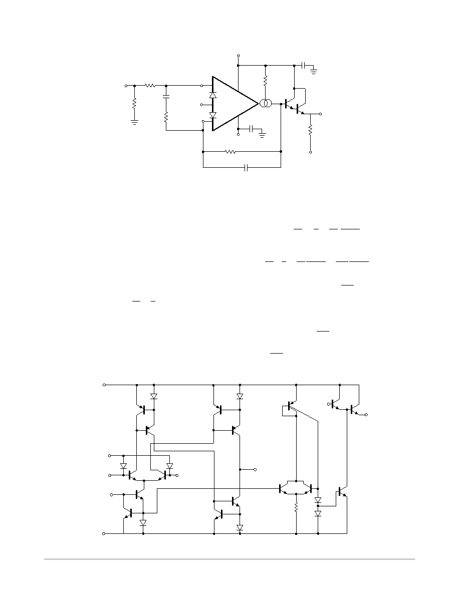
CIRCUIT DESCRIPTION
The circuit schematic diagram of one-half of the
AU5517/NE5517, a dual operational transconductance
amplifier with linearizing diodes and impedance buffers, is
shown in Figure 21.
Transconductance Amplifier
The transistor pair, Q4 and Q5, forms a transconductance
stage. The ratio of their collector currents (I4 and I5,
respectively) is defined by the differential input voltage, VIN,
which is shown in Equation 1.
VIN +
KT
q In
I5
I4
(eq. 1)
Where VIN is the difference of the two input voltages
KT
26 mV at room temperature (300°k).
Transistors Q1, Q2 and diode D1 form a current mirror which
focuses the sum of current I4 and I5 to be equal to amplifier bias
current IB:
I4 ) I5 + IB
(eq. 2)
If VIN is small, the ratio of I5 and I4 will approach unity and
the Taylor series of In function can be approximated as
KT
q In
I5
I4
[ KT
q
I5 * I4
I4
(eq. 3)
and I4 ^ I5 ^ IB
KT
q In
I5
I4
[ KT
q
I5 * I4
1 2IB
+ 2KT
q
I5 * I4
IB
+ VIN (eq. 4)
I5 * I4 + VIN
IB
q
2KT
The remaining transistors (Q6 to Q11) and diodes (D4 to D6)
form three current mirrors that produce an output current equal
to I5 minus I4. Thus:
VIN IB
q
2KT +
IO
(eq. 5)
The term
IB
q
2KT
is then the transconductance of the amplifier
and is proportional to IB.
Figure 21. Circuit Diagram of NE5517
V+
11
D4
Q6
Q7
2,15
D2
Q4
Q5
D3
INPUT
4,13
+INPUT
3,14
AMP BIAS
INPUT
1,16
Q2
Q1
D1
V
6
Q10
D6
Q11
VOUTPUT
5,12
Q9
Q8
D5
Q14
Q15
Q16
R1
D7
D8
Q3
7,10
Q12
Q13
8,9
相关PDF资料 |
PDF描述 |
|---|---|
| FWJ-18-01-T-S | CONN HEADER .156" 18POS SNGL TIN |
| 929648-01-36-I | CONN HEADER 36POS R/A .100" GOLD |
| CRCW04024R87FKED | RES 4.87 OHM 1/16W 1% 0402 SMD |
| SMS24CT1G | TVS ARRAY 5LINE 350W SC74-6 |
| NCV33274ADR2G | IC OPAMP QUAD HS BIPO 14-SOIC |
相关代理商/技术参数 |
参数描述 |
|---|---|
| NE5517D-T | 制造商:未知厂家 制造商全称:未知厂家 功能描述:Transconductance Operational Amplifier |
| NE5517N | 功能描述:跨导放大器 Transconductance RoHS:否 制造商:Texas Instruments 通道数量:1 封装 / 箱体:SOIC-14 带宽: 输入补偿电压:40 mV at +/- 5 V 电源电压-最大:+/- 5 V 电源电流: 最大工作温度:+ 85 C 最小工作温度:- 40 C 封装:Tube |
| NE5517NG | 功能描述:跨导放大器 Transconductance Dual Commercial Temp RoHS:否 制造商:Texas Instruments 通道数量:1 封装 / 箱体:SOIC-14 带宽: 输入补偿电压:40 mV at +/- 5 V 电源电压-最大:+/- 5 V 电源电流: 最大工作温度:+ 85 C 最小工作温度:- 40 C 封装:Tube |
| NE5520279A | 功能描述:射频MOSFET电源晶体管 L/S Band Med Power RoHS:否 制造商:Freescale Semiconductor 配置:Single 晶体管极性: 频率:1800 MHz to 2000 MHz 增益:27 dB 输出功率:100 W 汲极/源极击穿电压: 漏极连续电流: 闸/源击穿电压: 最大工作温度: 封装 / 箱体:NI-780-4 封装:Tray |
| NE5520279A-A | 功能描述:射频MOSFET电源晶体管 L/S Band Med Power RoHS:否 制造商:Freescale Semiconductor 配置:Single 晶体管极性: 频率:1800 MHz to 2000 MHz 增益:27 dB 输出功率:100 W 汲极/源极击穿电压: 漏极连续电流: 闸/源击穿电压: 最大工作温度: 封装 / 箱体:NI-780-4 封装:Tray |
发布紧急采购,3分钟左右您将得到回复。