参数资料
| 型号: | NE5517DR2G |
| 厂商: | ON Semiconductor |
| 文件页数: | 14/15页 |
| 文件大小: | 0K |
| 描述: | IC AMP XCONDUCTANCE DUAL 16-SOIC |
| 标准包装: | 1 |
| 放大器类型: | 跨导 |
| 电路数: | 2 |
| 输出类型: | 推挽式 |
| 转换速率: | 50 V/µs |
| 增益带宽积: | 2MHz |
| 电流 - 输入偏压: | 400nA |
| 电压 - 输入偏移: | 400µV |
| 电流 - 电源: | 2.6mA |
| 电流 - 输出 / 通道: | 650µA |
| 电压 - 电源,单路/双路(±): | 4 V ~ 44 V,±2 V ~ 22 V |
| 工作温度: | 0°C ~ 70°C |
| 安装类型: | 表面贴装 |
| 封装/外壳: | 16-SOIC(0.154",3.90mm 宽) |
| 供应商设备封装: | 16-SOIC |
| 包装: | 剪切带 (CT) |
| 其它名称: | NE5517DR2GOSCT |
NE5517, NE5517A, AU5517
http://onsemi.com
8
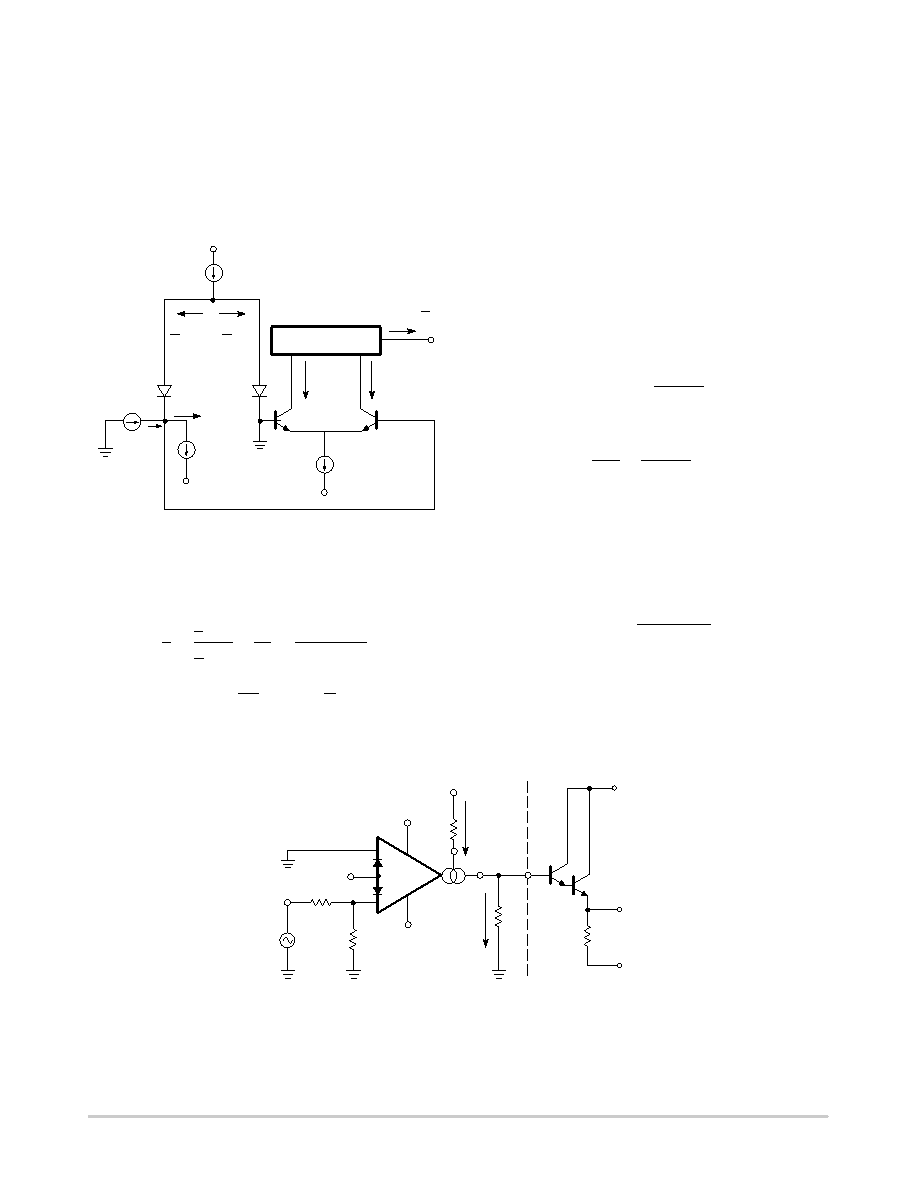
Linearizing Diodes
invalid and the transconductance increases non-linearly.
Figure 22 shows how the internal diodes can linearize the
transfer function of the operational amplifier. Assume D2
and D3 are biased with current sources and the input signal
current is IS. Since I4 + I5 = IB and I5 I4 = I0,
that is: I4 = (IB I0), I5 = (IB + I0)
+VS
ID
IB
I5
Q4
1/2ID
IS
1/2ID
VS
I4
I5
D3
D2
ID
2 * IS
ID
2 ) IS
I0 + I5 * I4
I0 + 2IS
IB
ID
Figure 22. Linearizing Diode
For the diodes and the input transistors that have identical
geometries and are subject to similar voltages and
temperatures, the following equation is true:
T
q In
ID
2 ) IS
ID
2 * IS
+ KT
q In
1 2(IB ) IO)
1 2(IB * IO)
(eq. 6)
IO + IS 2
I
B
ID
for |IS| t
ID
2
The only limitation is that the signal current should not
exceed ID.
Impedance Buffer
The upper limit of transconductance is defined by the
maximum value of IB (2.0 mA). The lowest value of IB for
which the amplifier will function therefore determines the
overall dynamic range. At low values of IB, a buffer with
very low input bias current is desired. A Darlington
amplifier with constant-current source (Q14, Q15, Q16, D7,
D8, and R1) suits the need.
APPLICATIONS
Voltage-Controlled Amplifier
input-voltage into small values (mV range) so the amplifier
operates in a linear manner.
It is:
IOUT +*VIN @
R3
R2 ) R3
@ gM;
VOUT + IOUT @ RL;
A +
VOUT
VIN
+
R3
R2 ) R3
@ gM @ RL
(3) gM = 19.2 IABC
(gM in mmhos for IABC in mA)
Since gM is directly proportional to IABC, the amplification
is controlled by the voltage VC in a simple way.
When VC is taken relative to VCC the following formula
is valid:
IABC +
(VC * 1.2V)
R1
The 1.2 V is the voltage across two base-emitter baths in
the current mirrors. This circuit is the base for many
applications of the AU5517/NE5517.
4
6
3
+
NE5517
5
11
1
7
8
VIN
R4 = R2/ /R3
+VCC
VC
R2
R3
R1
RL
RS
+VCC
INT
VOUT
VCC
IOUT
IABC
TYPICAL VALUES: R1 = 47kW
R2 = 10kW
R3 = 200W
R4 = 200W
RL = 100kW
RS = 47kW
INT
Figure 23.
相关PDF资料 |
PDF描述 |
|---|---|
| FWJ-18-01-T-S | CONN HEADER .156" 18POS SNGL TIN |
| 929648-01-36-I | CONN HEADER 36POS R/A .100" GOLD |
| CRCW04024R87FKED | RES 4.87 OHM 1/16W 1% 0402 SMD |
| SMS24CT1G | TVS ARRAY 5LINE 350W SC74-6 |
| NCV33274ADR2G | IC OPAMP QUAD HS BIPO 14-SOIC |
相关代理商/技术参数 |
参数描述 |
|---|---|
| NE5517D-T | 制造商:未知厂家 制造商全称:未知厂家 功能描述:Transconductance Operational Amplifier |
| NE5517N | 功能描述:跨导放大器 Transconductance RoHS:否 制造商:Texas Instruments 通道数量:1 封装 / 箱体:SOIC-14 带宽: 输入补偿电压:40 mV at +/- 5 V 电源电压-最大:+/- 5 V 电源电流: 最大工作温度:+ 85 C 最小工作温度:- 40 C 封装:Tube |
| NE5517NG | 功能描述:跨导放大器 Transconductance Dual Commercial Temp RoHS:否 制造商:Texas Instruments 通道数量:1 封装 / 箱体:SOIC-14 带宽: 输入补偿电压:40 mV at +/- 5 V 电源电压-最大:+/- 5 V 电源电流: 最大工作温度:+ 85 C 最小工作温度:- 40 C 封装:Tube |
| NE5520279A | 功能描述:射频MOSFET电源晶体管 L/S Band Med Power RoHS:否 制造商:Freescale Semiconductor 配置:Single 晶体管极性: 频率:1800 MHz to 2000 MHz 增益:27 dB 输出功率:100 W 汲极/源极击穿电压: 漏极连续电流: 闸/源击穿电压: 最大工作温度: 封装 / 箱体:NI-780-4 封装:Tray |
| NE5520279A-A | 功能描述:射频MOSFET电源晶体管 L/S Band Med Power RoHS:否 制造商:Freescale Semiconductor 配置:Single 晶体管极性: 频率:1800 MHz to 2000 MHz 增益:27 dB 输出功率:100 W 汲极/源极击穿电压: 漏极连续电流: 闸/源击穿电压: 最大工作温度: 封装 / 箱体:NI-780-4 封装:Tray |
发布紧急采购,3分钟左右您将得到回复。