- 您现在的位置:买卖IC网 > PDF目录17493 > NTB60N06LT4 (ON Semiconductor)MOSFET N-CH 60V 60A D2PAK PDF资料下载
参数资料
| 型号: | NTB60N06LT4 |
| 厂商: | ON Semiconductor |
| 文件页数: | 4/8页 |
| 文件大小: | 0K |
| 描述: | MOSFET N-CH 60V 60A D2PAK |
| 产品变化通告: | Product Obsolescence 11/Feb/2009 |
| 标准包装: | 800 |
| FET 型: | MOSFET N 通道,金属氧化物 |
| FET 特点: | 逻辑电平门 |
| 漏极至源极电压(Vdss): | 60V |
| 电流 - 连续漏极(Id) @ 25° C: | 60A |
| 开态Rds(最大)@ Id, Vgs @ 25° C: | 16 毫欧 @ 30A,5V |
| Id 时的 Vgs(th)(最大): | 2V @ 250µA |
| 闸电荷(Qg) @ Vgs: | 65nC @ 5V |
| 输入电容 (Ciss) @ Vds: | 3075pF @ 25V |
| 功率 - 最大: | 2.4W |
| 安装类型: | 表面贴装 |
| 封装/外壳: | TO-263-3,D²Pak(2 引线+接片),TO-263AB |
| 供应商设备封装: | D2PAK |
| 包装: | 带卷 (TR) |
| 其它名称: | NTB60N06LT4OS |
�� �
�
�NTP60N06L,� NTB60N06L�
�POWER� MOSFET� SWITCHING�
�Switching� behavior� is� most� easily� modeled� and� predicted�
�by� recognizing� that� the� power� MOSFET� is� charge�
�controlled.� The� lengths� of� various� switching� intervals� (� D� t)�
�are� determined� by� how� fast� the� FET� input� capacitance� can�
�be� charged� by� current� from� the� generator.�
�The� published� capacitance� data� is� difficult� to� use� for�
�calculating� rise� and� fall� because� drain?gate� capacitance�
�varies� greatly� with� applied� voltage.� Accordingly,� gate�
�charge� data� is� used.� In� most� cases,� a� satisfactory� estimate� of�
�average� input� current� (I� G(AV)� )� can� be� made� from� a�
�rudimentary� analysis� of� the� drive� circuit� so� that�
�t� =� Q/I� G(AV)�
�During� the� rise� and� fall� time� interval� when� switching� a�
�resistive� load,� V� GS� remains� virtually� constant� at� a� level�
�known� as� the� plateau� voltage,� V� SGP� .� Therefore,� rise� and� fall�
�times� may� be� approximated� by� the� following:�
�t� r� =� Q� 2� x� R� G� /(V� GG� ?� V� GSP� )�
�t� f� =� Q� 2� x� R� G� /V� GSP�
�where�
�V� GG� =� the� gate� drive� voltage,� which� varies� from� zero� to� V� GG�
�R� G� =� the� gate� drive� resistance�
�and� Q� 2� and� V� GSP� are� read� from� the� gate� charge� curve.�
�During� the� turn?on� and� turn?off� delay� times,� gate� current� is�
�not� constant.� The� simplest� calculation� uses� appropriate�
�values� from� the� capacitance� curves� in� a� standard� equation� for�
�voltage� change� in� an� RC� network.� The� equations� are:�
�t� d(on)� =� R� G� C� iss� In� [V� GG� /(V� GG� ?� V� GSP� )]�
�t� d(off)� =� R� G� C� iss� In� (V� GG� /V� GSP� )�
�8000�
�The� capacitance� (C� iss� )� is� read� from� the� capacitance� curve� at�
�a� voltage� corresponding� to� the� off?state� condition� when�
�calculating� t� d(on)� and� is� read� at� a� voltage� corresponding� to� the�
�on?state� when� calculating� t� d(off)� .�
�At� high� switching� speeds,� parasitic� circuit� elements�
�complicate� the� analysis.� The� inductance� of� the� MOSFET�
�source� lead,� inside� the� package� and� in� the� circuit� wiring�
�which� is� common� to� both� the� drain� and� gate� current� paths,�
�produces� a� voltage� at� the� source� which� reduces� the� gate� drive�
�current.� The� voltage� is� determined� by� Ldi/dt,� but� since� di/dt�
�is� a� function� of� drain� current,� the� mathematical� solution� is�
�complex.� The� MOSFET� output� capacitance� also�
�complicates� the� mathematics.� And� finally,� MOSFETs� have�
�finite� internal� gate� resistance� which� effectively� adds� to� the�
�resistance� of� the� driving� source,� but� the� internal� resistance�
�is� difficult� to� measure� and,� consequently,� is� not� specified.�
�The� resistive� switching� time� variation� versus� gate�
�resistance� (Figure� 9)� shows� how� typical� switching�
�performance� is� affected� by� the� parasitic� circuit� elements.� If�
�the� parasitics� were� not� present,� the� slope� of� the� curves� would�
�maintain� a� value� of� unity� regardless� of� the� switching� speed.�
�The� circuit� used� to� obtain� the� data� is� constructed� to� minimize�
�common� inductance� in� the� drain� and� gate� circuit� loops� and�
�is� believed� readily� achievable� with� board� mounted�
�components.� Most� power� electronic� loads� are� inductive;� the�
�data� in� the� figure� is� taken� with� a� resistive� load,� which�
�approximates� an� optimally� snubbed� inductive� load.� Power�
�MOSFETs� may� be� safely� operated� into� an� inductive� load;�
�however,� snubbing� reduces� switching� losses.�
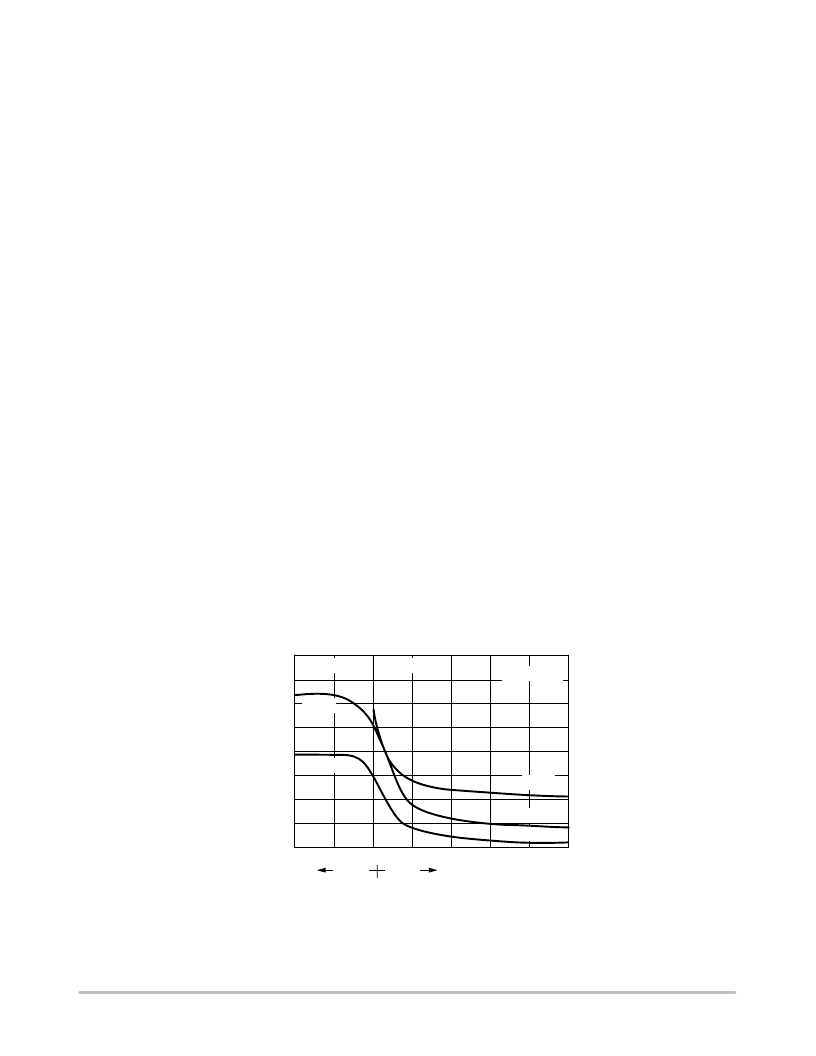
�6000�
�V� DS� =� 0� V�
�C� iss�
�V� GS� =� 0� V�
�T� J� =� 25� °� C�
�4000�
�C� rss�
�C� iss�
�2000�
�C� oss�
�C� rss�
�0�
�10�
�5�
�0�
�5�
�10�
�15�
�20�
�25�
�V� GS�
�V� DS�
�GATE?TO?SOURCE� OR� DRAIN?TO?SOURCE� VOLTAGE� (VOLTS)�
�Figure� 7.� Capacitance� Variation�
�http://onsemi.com�
�4�
�相关PDF资料 |
PDF描述 |
|---|---|
| NTB18N06LT4 | MOSFET N-CH 60V 15A D2PAK |
| NTB18N06T4 | MOSFET N-CH 60V 15A D2PAK |
| NTF3055L108T3LF | MOSFET N-CH 60V 3A SOT223 |
| NIF9N05CLT3 | MOSFET N-CH 52V 2.6A SOT223 |
| NTB30N06LT4 | MOSFET N-CH 60V 30A D2PAK |
相关代理商/技术参数 |
参数描述 |
|---|---|
| NTB60N06LT4G | 功能描述:MOSFET 60V 60A N-Channel RoHS:否 制造商:STMicroelectronics 晶体管极性:N-Channel 汲极/源极击穿电压:650 V 闸/源击穿电压:25 V 漏极连续电流:130 A 电阻汲极/源极 RDS(导通):0.014 Ohms 配置:Single 最大工作温度: 安装风格:Through Hole 封装 / 箱体:Max247 封装:Tube |
| NTB60N06T4 | 功能描述:MOSFET 60V 60A N-Channel RoHS:否 制造商:STMicroelectronics 晶体管极性:N-Channel 汲极/源极击穿电压:650 V 闸/源击穿电压:25 V 漏极连续电流:130 A 电阻汲极/源极 RDS(导通):0.014 Ohms 配置:Single 最大工作温度: 安装风格:Through Hole 封装 / 箱体:Max247 封装:Tube |
| NTB60N06T4G | 功能描述:MOSFET 60V 60A N-Channel RoHS:否 制造商:STMicroelectronics 晶体管极性:N-Channel 汲极/源极击穿电压:650 V 闸/源击穿电压:25 V 漏极连续电流:130 A 电阻汲极/源极 RDS(导通):0.014 Ohms 配置:Single 最大工作温度: 安装风格:Through Hole 封装 / 箱体:Max247 封装:Tube |
| NTB6410AN | 制造商:ONSEMI 制造商全称:ON Semiconductor 功能描述:N-Channel Power MOSFET 100 V, 76 A, 13 mΩ |
| NTB6410ANG | 功能描述:MOSFET NFET D2PAK 100V 76A 13MOH RoHS:否 制造商:STMicroelectronics 晶体管极性:N-Channel 汲极/源极击穿电压:650 V 闸/源击穿电压:25 V 漏极连续电流:130 A 电阻汲极/源极 RDS(导通):0.014 Ohms 配置:Single 最大工作温度: 安装风格:Through Hole 封装 / 箱体:Max247 封装:Tube |
发布紧急采购,3分钟左右您将得到回复。