- 您现在的位置:买卖IC网 > PDF目录363711 > NTGS3443T1 (ON SEMICONDUCTOR) Power MOSFET 2 Amp, 20 Volts P-Channel TSOP-6(2A,20V,P通道,TSOP-6封装的功率MOSFET) PDF资料下载
参数资料
| 型号: | NTGS3443T1 |
| 厂商: | ON SEMICONDUCTOR |
| 元件分类: | 小信号晶体管 |
| 英文描述: | Power MOSFET 2 Amp, 20 Volts P-Channel TSOP-6(2A,20V,P通道,TSOP-6封装的功率MOSFET) |
| 中文描述: | 2200 mA, 20 V, P-CHANNEL, Si, SMALL SIGNAL, MOSFET |
| 封装: | MINIATURE, CASE 318G-02, TSOP-6 |
| 文件页数: | 1/6页 |
| 文件大小: | 136K |
| 代理商: | NTGS3443T1 |
Semiconductor Components Industries, LLC, 2006
February, 2006
Rev. 3
1
Publication Order Number:
NTGS3443T1/D
NTGS3443T1
Power MOSFET
2 Amps, 20 Volts
P
Channel TSOP
6
Features
Ultra Low R
DS(on)
Higher Efficiency Extending Battery Life
Miniature TSOP
6 Surface Mount Package
Pb
Free Package is Available
Applications
Power Management in Portable and Battery
Powered Products,
i.e.: Cellular and Cordless Telephones, and PCMCIA Cards
MAXIMUM RATINGS
(T
J
= 25
°
C unless otherwise noted)
Rating
Symbol
Value
Unit
Drain
to
Source Voltage
Gate
to
Source Voltage
Continuous
Thermal Resistance
Junction
to
Ambient (Note 1)
Total Power Dissipation @ T
A
= 25
°
C
Drain Current
Continuous @ T
A
= 25
°
C
Pulsed Drain Current (T
p
Thermal Resistance
Junction
to
Ambient (Note 2)
Total Power Dissipation @ T
A
= 25
°
C
Drain Current
Continuous @ T
A
= 25
°
C
Pulsed Drain Current (T
p
Thermal Resistance
Junction
to
Ambient (Note 3)
Total Power Dissipation @ T
A
= 25
°
C
Drain Current
Continuous @ T
A
= 25
°
C
Pulsed Drain Current (T
p
Operating and Storage Temperature Range
V
DSS
V
GS
20
12
Volts
Volts
10 S)
R
JA
P
d
I
D
I
DM
244
0.5
2.2
10
°
C/W
Watts
Amps
Amps
10 S)
R
JA
P
d
I
D
I
DM
128
1.0
3.1
14
°
C/W
Watts
Amps
Amps
10 S)
R
JA
P
d
I
D
I
DM
62.5
2.0
4.4
20
°
C/W
Watts
Amps
Amps
T
J
, T
stg
55 to
150
260
°
C
Maximum Lead Temperature for Soldering
Purposes for 10 Seconds
Maximum ratings are those values beyond which device damage can occur.
Maximum ratings applied to the device are individual stress limit values (not
normal operating conditions) and are not valid simultaneously. If these limits are
exceeded, device functional operation is not implied, damage may occur and
reliability may be affected.
1. Minimum FR
4 or G
10 PCB, operating to steady state.
2. Mounted onto a 2 in square FR
4 board (1 in sq, 2 oz. Cu. 0.06
″
thick single
sided), operating to steady state.
3. Mounted onto a 2 in square FR
4 board (1 in sq, 2 oz. Cu. 0.06
″
thick single
sided), t
5.0 seconds.
T
L
°
C
2 AMPERES
20 VOLTS
R
DS(on)
= 65 m
3
4
1 2 5 6
Device
Package
Shipping
ORDERING INFORMATION
NTGS3443T1
TSOP
6
3000 Tape & Reel
P
Channel
NTGS3443T1G
TSOP
6
3000 Tape & Reel
For information on tape and reel specifications,
including part orientation and tape sizes, please
refer to our Tape and Reel Packaging Specifications
Brochure, BRD8011/D.
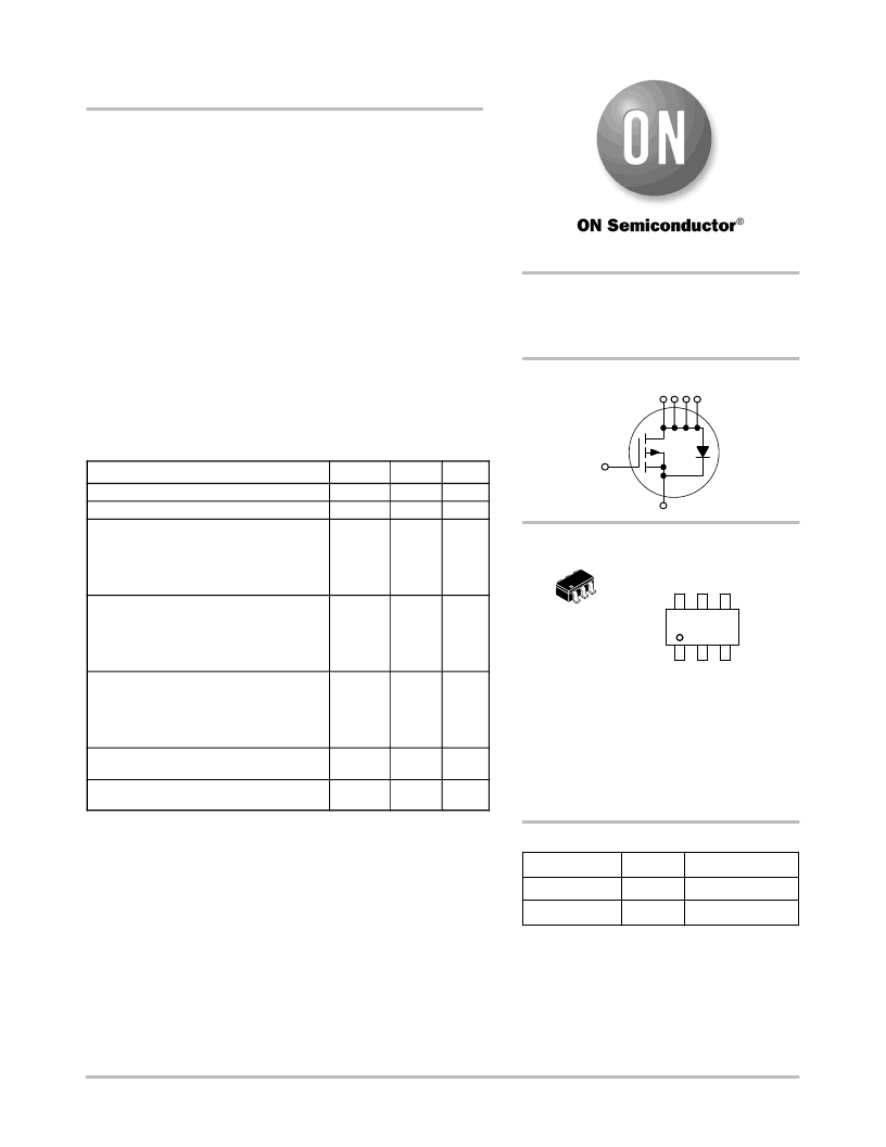
TSOP
6
CASE 318G
STYLE 1
MARKING DIAGRAM &
PIN ASSIGNMENT
1
443
M
= Specific Device Code
= Date Code*
= Pb
Free Package
Source
4
Drain
6
Drain
5
3
Gate
1
Drain
2
Drain
(Note: Microdot may be in either location)
* Date Code orientation may vary depending
upon manufacturing location.
443 M
http://onsemi.com
相关PDF资料 |
PDF描述 |
|---|---|
| NTGS3446 | Power MOSFET 5.1 Amps, 20 Volts N-Channel TSOP-6(5.1A,20V逻辑电平,N通道,TSOP-6封装的功率MOSFET) |
| NTGS3455T1 | MOSFET -3.5 Amps, -30 Volts P-Channel TSOP-6(-3.5A,-30V,P通道,TSOP-6封装的MOSFET) |
| NTHC5513 | Power MOSFET(功率MOSFET) |
| NTHD3100C | Power MOSFET 20V, +3.9A/4.4A, Complementary ChipFET(20V, +3.9A/4.4A功率MOSFET) |
| NTHD3101F | Power MOSFET and Schottky Diode(20V, 4.4A功率MOSFET) |
相关代理商/技术参数 |
参数描述 |
|---|---|
| NTGS3443T1/D | 制造商:未知厂家 制造商全称:未知厂家 功能描述:Power MOSFET 2 Amps, 20 Volts |
| NTGS3443T1G | 功能描述:MOSFET 20V 2A P-Channel RoHS:否 制造商:STMicroelectronics 晶体管极性:N-Channel 汲极/源极击穿电压:650 V 闸/源击穿电压:25 V 漏极连续电流:130 A 电阻汲极/源极 RDS(导通):0.014 Ohms 配置:Single 最大工作温度: 安装风格:Through Hole 封装 / 箱体:Max247 封装:Tube |
| NTGS3443T1G | 制造商:ON Semiconductor 功能描述:MOSFET |
| NTGS3443T2G | 功能描述:MOSFET PFET 20V 0.10R TR RoHS:否 制造商:STMicroelectronics 晶体管极性:N-Channel 汲极/源极击穿电压:650 V 闸/源击穿电压:25 V 漏极连续电流:130 A 电阻汲极/源极 RDS(导通):0.014 Ohms 配置:Single 最大工作温度: 安装风格:Through Hole 封装 / 箱体:Max247 封装:Tube |
| NTGS3446 | 制造商:ONSEMI 制造商全称:ON Semiconductor 功能描述:Power MOSFET 5.1 Amps, 20 Volts N−Channel TSOP−6 |
发布紧急采购,3分钟左右您将得到回复。