- 您现在的位置:买卖IC网 > Datasheet目录489 > NTHD5903T1G (ON Semiconductor)MOSFET PWR P-CH DUAL20V CHIPFET Datasheet资料下载
参数资料
| 型号: | NTHD5903T1G |
| 厂商: | ON Semiconductor |
| 文件页数: | 1/6页 |
| 文件大小: | 0K |
| 描述: | MOSFET PWR P-CH DUAL20V CHIPFET |
| 产品变化通告: | Product Obsolescence 21/Jan/2010 |
| 标准包装: | 1 |
| FET 型: | 2 个 P 沟道(双) |
| FET 特点: | 逻辑电平门 |
| 漏极至源极电压(Vdss): | 20V |
| 电流 - 连续漏极(Id) @ 25° C: | 2.2A |
| 开态Rds(最大)@ Id, Vgs @ 25° C: | 155 毫欧 @ 2.2A,4.5V |
| Id 时的 Vgs(th)(最大): | 600mV @ 250µA |
| 闸电荷(Qg) @ Vgs: | 7.4nC @ 4.5V |
| 功率 - 最大: | 1.1W |
| 安装类型: | 表面贴装 |
| 封装/外壳: | 8-SMD,扁平引线 |
| 供应商设备封装: | ChipFET? |
| 包装: | 剪切带 (CT) |
| 其它名称: | NTHD5903T1GOSCT |
�� �
�
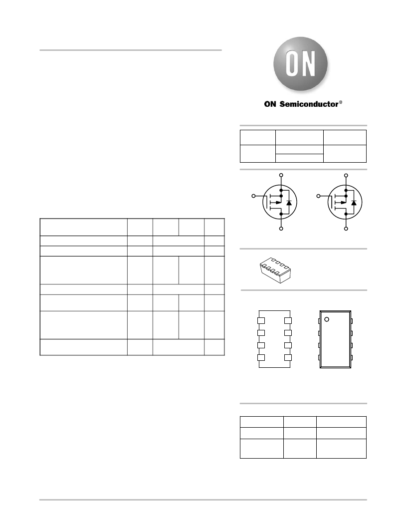
�NTHD5903�
�Power� MOSFET�
�?20� V,� ?3.0� A,� Dual� P?Channel� ChipFET� E�
�Features�
�?� Low� R� DS(on)� for� Higher� Efficiency�
�?� Logic� Level� Gate� Drive�
�?� Miniature� ChipFET� Surface� Mount� Package� Saves� Board� Space�
�?� Pb?Free� Package� is� Available�
�Applications�
�?� Power� Management� in� Portable� and� Battery?Powered� Products;�
�i.e.,� Cellular� and� Cordless� Telephones� and� PCMCIA� Cards�
�V� (BR)DSS�
�?20� V�
�G1�
�http://onsemi.com�
�R� DS(on)� TYP�
�130� m� W� @� ?4.5� V�
�215� m� W� @� ?2.5� V�
�S1�
�G2�
�I� D� MAX�
�?3.0� A�
�S2�
�MAXIMUM� RATINGS� (T� A� =� 25� °� C� unless� otherwise� noted)�
�Steady�
�Rating�
�Drain?Source� Voltage�
�Symbol�
�V� DS�
�5� secs�
�?20�
�State�
�Unit�
�V�
�D1�
�P?Channel� MOSFET�
�D2�
�P?Channel� MOSFET�
�Gate?Source� Voltage�
�V� GS�
�"� 12�
�V�
�Continuous� Drain� Current�
�(T� J� =� 150� °� C)� (Note� 1)�
�T� A� =� 25� °� C�
�T� A� =� 85� °� C�
�Pulsed� Drain� Current�
�I� D�
�I� DM�
�"� 3.0�
�"� 2.2�
�"� 10�
�"� 2.2�
�"� 1.6�
�A�
�A�
�ChipFET�
�CASE� 1206A�
�STYLE� 2�
�Continuous� Source� Current�
�(Diode� Conduction)� (Note� 1)�
�I� S�
�?3.0�
�?2.2�
�A�
�PIN�
�CONNECTIONS�
�MARKING�
�DIAGRAM�
�Maximum� Power� Dissipation�
�(Note� 1)�
�T� A� =� 25� °� C�
�T� A� =� 85� °� C�
�P� D�
�2.1�
�1.1�
�1.1�
�0.6�
�W�
�D� 1� 8�
�D� 1� 7�
�1� S� 1�
�2� G� 1�
�1�
�2�
�8�
�7�
�Operating� Junction� and� Storage�
�Temperature� Range�
�T� J� ,� T� stg�
�?55� to� +150�
�°� C�
�D� 2� 6�
�3� S� 2�
�3�
�6�
�Maximum� ratings� are� those� values� beyond� which� device� damage� can� occur.�
�D� 2� 5�
�4� G� 2�
�4�
�5�
�Maximum� ratings� applied� to� the� device� are� individual� stress� limit� values� (not�
�normal� operating� conditions)� and� are� not� valid� simultaneously.� If� these� limits� are�
�exceeded,� device� functional� operation� is� not� implied,� damage� may� occur� and�
�reliability� may� be� affected.�
�1.� Surface� Mounted� on� FR4� Board� using� 1� in� sq� pad� size� (Cu� area� =� 1.27� in� sq�
�[1� oz]� including� traces).�
�A7� =� Specific� Device� Code�
�M� =� Month� Code�
�G� =� Pb?Free� Package�
�ORDERING� INFORMATION�
�Device�
�NTHD5903T1�
�NTHD5903T1G�
�Package�
�ChipFET�
�ChipFET�
�Shipping� ?�
�3000/Tape� &� Reel�
�3000/Tape� &� Reel�
�(Pb?Free)�
�?For� information� on� tape� and� reel� specifications,�
�including� part� orientation� and� tape� sizes,� please�
�refer� to� our� Tape� and� Reel� Packaging� Specifications�
�Brochure,� BRD8011/D.�
�?� Semiconductor� Components� Industries,� LLC,� 2005�
�November,� 2005� ?� Rev.� 4�
�1�
�Publication� Order� Number:�
�NTHD5903/D�
�相关PDF资料 |
PDF描述 |
|---|---|
| NTHD5904NT1G | MOSFET N-CHAN 3.3A 20V CHIPFET |
| NTHS2101PT1 | MOSFET P-CH 8V 5.4A CHIPFET |
| NTHS4101PT1G | MOSFET P-CH 20V 4.8A CHIPFET |
| NTHS4166NT1G | MOSFET N-CH 30V 4.9A CHIPFET |
| NTHS4501NT1G | MOSFET N-CH 30V 4.9A CHIPFET |
相关代理商/技术参数 |
参数描述 |
|---|---|
| NTHD5904N | 制造商:ONSEMI 制造商全称:ON Semiconductor 功能描述:Power MOSFET 20 V, 4.5 A, Dual N−Channel, ChipFET |
| NTHD5904N_05 | 制造商:ONSEMI 制造商全称:ON Semiconductor 功能描述:Power MOSFET 20 V, 4.5 A, Dual N−Channel, ChipFET |
| NTHD5904NT1 | 功能描述:MOSFET 20V 4.5A Dual RoHS:否 制造商:STMicroelectronics 晶体管极性:N-Channel 汲极/源极击穿电压:650 V 闸/源击穿电压:25 V 漏极连续电流:130 A 电阻汲极/源极 RDS(导通):0.014 Ohms 配置:Single 最大工作温度: 安装风格:Through Hole 封装 / 箱体:Max247 封装:Tube |
| NTHD5904NT1G | 功能描述:MOSFET 20V 4.5A Dual N-Channel RoHS:否 制造商:STMicroelectronics 晶体管极性:N-Channel 汲极/源极击穿电压:650 V 闸/源击穿电压:25 V 漏极连续电流:130 A 电阻汲极/源极 RDS(导通):0.014 Ohms 配置:Single 最大工作温度: 安装风格:Through Hole 封装 / 箱体:Max247 封装:Tube |
| NTHD5904NT3 | 功能描述:MOSFET 20V 4.5A Dual RoHS:否 制造商:STMicroelectronics 晶体管极性:N-Channel 汲极/源极击穿电压:650 V 闸/源击穿电压:25 V 漏极连续电流:130 A 电阻汲极/源极 RDS(导通):0.014 Ohms 配置:Single 最大工作温度: 安装风格:Through Hole 封装 / 箱体:Max247 封装:Tube |
发布紧急采购,3分钟左右您将得到回复。