- 您现在的位置:买卖IC网 > Datasheet目录490 > NTLJS2103PTAG (ON Semiconductor)MOSFET P-CH 12V 3.5A 6-WDFN Datasheet资料下载
参数资料
| 型号: | NTLJS2103PTAG |
| 厂商: | ON Semiconductor |
| 文件页数: | 1/6页 |
| 文件大小: | 0K |
| 描述: | MOSFET P-CH 12V 3.5A 6-WDFN |
| 产品变化通告: | Product Obsolescence 14/Apr/2010 |
| 标准包装: | 3,000 |
| FET 型: | MOSFET P 通道,金属氧化物 |
| FET 特点: | 逻辑电平门 |
| 漏极至源极电压(Vdss): | 12V |
| 电流 - 连续漏极(Id) @ 25° C: | 3.5A |
| 开态Rds(最大)@ Id, Vgs @ 25° C: | 40 毫欧 @ 3A,4.5V |
| Id 时的 Vgs(th)(最大): | 800mV @ 250µA |
| 闸电荷(Qg) @ Vgs: | 15nC @ 4.5V |
| 输入电容 (Ciss) @ Vds: | 1157pF @ 6V |
| 功率 - 最大: | 700mW |
| 安装类型: | 表面贴装 |
| 封装/外壳: | 6-WDFN 裸露焊盘 |
| 供应商设备封装: | 6-WDFN(2x2) |
| 包装: | 带卷 (TR) |
�� �
�
�NTLJS2103P�
�Power� MOSFET�
�?� 12� V,� ?� 7.7� A,� m� Cool� t� Single� P� ?� Channel,�
�2x2� mm,� WDFN� Package�
�Features�
�?� Recommended Replacement Device� ?� NTLUS3A40P�
�?� WDFN� Package� Provides� Exposed� Drain� Pad� for� Excellent� Thermal�
�Conduction�
�?� 2x2� mm� Footprint� Same� as� SC� ?� 88� Package�
�?� Lowest� R� DS(on)� Solution� in� 2x2� mm� Package�
�?� 1.2� V� R� DS(on)� Rating� for� Operation� at� Low� Voltage� Logic� Level� Gate�
�Drive�
�?� Low� Profile� (<� 0.8� mm)� for� Easy� Fit� in� Thin� Environments�
�?� These� Devices� are� Pb� ?� Free,� Halogen� Free/BFR� Free� and� are� RoHS�
�Compliant�
�V� (BR)DSS�
�?� 12� V�
�http://onsemi.com�
�R� DS(on)� TYP� I� D� MAX� (Note� 1)�
�25� m� W� @� ?� 4.5� V� ?� 5.9� A�
�35� m� W� @� ?� 2.5� V� ?� 5.3� A�
�45� m� W� @� ?� 1.8� V� ?� 2.0� A�
�60� m� W� @� ?� 1.5� V� ?� 1.0� A�
�95� m� W� @� ?� 1.2� V� ?� 0.2� A�
�S�
�Applications�
�?� High� Side� Load� Switch�
�?� DC� ?� DC� Converters� (Buck� and� Boost� Circuits)�
�?� Optimized� for� Battery� and� Load� Management� Applications� in�
�Portable� Equipment�
�?� Li� ?� Ion� Battery� Linear� Mode� Charging�
�MAXIMUM� RATINGS� (T� J� =� 25� °� C� unless� otherwise� noted)�
�G�
�S�
�D�
�D�
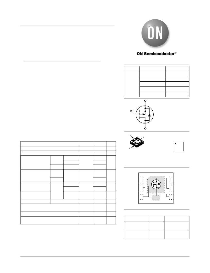
�P� ?� CHANNEL� MOSFET�
�MARKING�
�DIAGRAM�
�Steady�
�State�
�1�
�6�
�Parameter�
�Drain� ?� to� ?� Source� Voltage�
�Gate� ?� to� ?� Source� Voltage�
�Continuous� Drain�
�Current� (Note� 1)�
�t� ≤� 5s�
�Power� Dissipation� Steady�
�(Note� 1)� State�
�t� ≤� 5s�
�T� A� =� 25� °� C�
�T� A� =� 85� °� C�
�T� A� =� 25� °� C�
�T� A� =� 25� °� C�
�Symbol�
�V� DSS�
�V� GS�
�I� D�
�P� D�
�Value�
�?� 12�
�±� 8.0�
�?� 5.9�
�?� 4.2�
�?� 7.7�
�1.9�
�3.3�
�Unit�
�V�
�V�
�A�
�W�
�Pin� 1�
�D�
�WDFN6� 1� 6�
�CASE� 506AP� 2� J7M� G� 5�
�3� G� 4�
�J7� =� Specific� Device� Code�
�M� =� Date� Code�
�G� =� Pb� ?� Free� Package�
�(Note:� Microdot� may� be� in� either� location)�
�PIN� CONNECTIONS�
�D�
�Continuous� Drain�
�Current� (Note� 2)�
�Power� Dissipation�
�(Note� 2)�
�Pulsed� Drain� Current�
�T� A� =� 25� °� C�
�Steady� T� A� =� 85� °� C�
�State�
�T� A� =� 25� °� C�
�t� p� =� 10� m� s�
�I� D�
�P� D�
�I� DM�
�?� 3.5�
�?� 2.5�
�0.7�
�?� 24�
�A�
�W�
�A�
�D�
�G�
�2�
�3�
�S�
�D�
�5�
�4�
�D�
�S�
�Operating� Junction� and� Storage� Temperature�
�Source� Current� (Body� Diode)� (Note� 2)�
�T� J� ,� T� STG�
�I� S�
�?� 55� to�
�150�
�?� 2.7�
�°� C�
�A�
�(Top� View)�
�ORDERING� INFORMATION�
�Lead� Temperature� for� Soldering� Purposes� T� L� 260� °� C�
�(1/8� ″� from� case� for� 10� s)�
�Stresses� exceeding� Maximum� Ratings� may� damage� the� device.� Maximum�
�Ratings� are� stress� ratings� only.� Functional� operation� above� the� Recommended�
�Operating� Conditions� is� not� implied.� Extended� exposure� to� stresses� above� the�
�Recommended� Operating� Conditions� may� affect� device� reliability.�
�Device�
�NTLJS2103PTAG�
�NTLJS2103PTBG�
�Package�
�WDFN6�
�(Pb� ?� Free)�
�WDFN6�
�(Pb� ?� Free)�
�Shipping� ?�
�3000/Tape� &� Reel�
�3000/Tape� &� Reel�
�1.� Surface� Mounted� on� FR4� Board� using� 1� in� sq� pad� size� (Cu� area� =� 1.127� in� sq�
�[2� oz]� including� traces).�
�2.� Surface� Mounted� on� FR4� Board� using� the� minimum� recommended� pad� size,�
�(30� mm� 2� ,� 2� oz� Cu).�
�?For� information� on� tape� and� reel� specifications,�
�including� part� orientation� and� tape� sizes,� please�
�refer� to� our� Tape� and� Reel� Packaging� Specification�
�Brochure,� BRD8011/D.�
�?� Semiconductor� Components� Industries,� LLC,� 2011�
�March,� 2011� ?� Rev.� 3�
�1�
�Publication� Order� Number:�
�NTLJS2103P/D�
�相关PDF资料 |
PDF描述 |
|---|---|
| NTLJS3113PTAG | MOSFET P-CH 20V 3.5A 6-WDFN |
| NTLJS3180PZTBG | MOSFET P-CH 20V 3.5A 6-WDFN |
| NTLJS4114NT1G | MOSFET N-CH 30V 3.6A 6-WDFN |
| NTLJS4149PTBG | MOSFET P-CH 30V 4.6A SGL 6WDFN |
| NTLJS4159NT1G | MOSFET N-CH 30V 3.6A 6-WFDN |
相关代理商/技术参数 |
参数描述 |
|---|---|
| NTLJS2103PTBG | 功能描述:MOSFET PFET WDFN6 12V 5.9A 0.025 RoHS:否 制造商:STMicroelectronics 晶体管极性:N-Channel 汲极/源极击穿电压:650 V 闸/源击穿电压:25 V 漏极连续电流:130 A 电阻汲极/源极 RDS(导通):0.014 Ohms 配置:Single 最大工作温度: 安装风格:Through Hole 封装 / 箱体:Max247 封装:Tube |
| NTLJS3113P | 制造商:ONSEMI 制造商全称:ON Semiconductor 功能描述:Power MOSFET −20 V, −7.7 A, uCool TM Single 2x2 mm, WDFN Package |
| NTLJS3113P_06 | 制造商:ONSEMI 制造商全称:ON Semiconductor 功能描述:Power MOSFET −20 V, −7.7 A, uCool TM Single 2x2 mm, WDFN Package |
| NTLJS3113PT1G | 功能描述:MOSFET PFET 2X2 20V 9.5A 42MOHM RoHS:否 制造商:STMicroelectronics 晶体管极性:N-Channel 汲极/源极击穿电压:650 V 闸/源击穿电压:25 V 漏极连续电流:130 A 电阻汲极/源极 RDS(导通):0.014 Ohms 配置:Single 最大工作温度: 安装风格:Through Hole 封装 / 箱体:Max247 封装:Tube |
| NTLJS3113PTAG | 功能描述:MOSFET PFET 20V 9.5A 42MOHM 2X2 RoHS:否 制造商:STMicroelectronics 晶体管极性:N-Channel 汲极/源极击穿电压:650 V 闸/源击穿电压:25 V 漏极连续电流:130 A 电阻汲极/源极 RDS(导通):0.014 Ohms 配置:Single 最大工作温度: 安装风格:Through Hole 封装 / 箱体:Max247 封装:Tube |
发布紧急采购,3分钟左右您将得到回复。