- 您现在的位置:买卖IC网 > Datasheet目录492 > NTMSD3P303R2G (ON Semiconductor)MOSFET P-CH 30V 2.34A 8-SOIC Datasheet资料下载
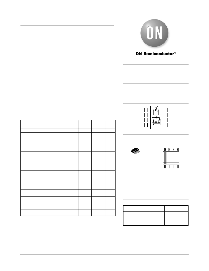
参数资料
| 型号: | NTMSD3P303R2G |
| 厂商: | ON Semiconductor |
| 文件页数: | 1/9页 |
| 文件大小: | 0K |
| 描述: | MOSFET P-CH 30V 2.34A 8-SOIC |
| 产品变化通告: | Product Obsolescence 13/Apr/2009 |
| 标准包装: | 2,500 |
| 系列: | FETKY™ |
| FET 型: | MOSFET P 通道,金属氧化物 |
| FET 特点: | 二极管(隔离式) |
| 漏极至源极电压(Vdss): | 30V |
| 电流 - 连续漏极(Id) @ 25° C: | 2.34A |
| 开态Rds(最大)@ Id, Vgs @ 25° C: | 85 毫欧 @ 3.05A,10V |
| Id 时的 Vgs(th)(最大): | 2.5V @ 250µA |
| 闸电荷(Qg) @ Vgs: | 25nC @ 10V |
| 输入电容 (Ciss) @ Vds: | 750pF @ 24V |
| 功率 - 最大: | 730mW |
| 安装类型: | 表面贴装 |
| 封装/外壳: | 8-SOIC(0.154",3.90mm 宽) |
| 供应商设备封装: | 8-SOICN |
| 包装: | 带卷 (TR) |
| 其它名称: | NTMSD3P303R2GOS |
�� �
�
�NTMSD3P303R2�
�FETKY� ?�
�P� ?� Channel� Enhancement� ?� Mode�
�Power� MOSFET� and� Schottky� Diode�
�Dual� SO� ?� 8� Package�
�3�
�Features�
�?� High� Efficiency� Components� in� a� Single� SO� ?� 8� Package�
�?� High� Density� Power� MOSFET� with� Low� R� DS(on)� ,�
�Schottky� Diode� with� Low� V� F�
�?� Independent� Pin� ?� Outs� for� MOSFET� and� Schottky� Die�
�Allowing� for� Flexibility� in� Application� Use�
�?� Less� Component� Placement� for� Board� Space� Savings�
�?� SO� ?� 8� Surface� Mount� Package,�
�Mounting� Information� for� SO� ?� 8� Package� Provided�
�?� Pb� ?� Free� Package� is� Available�
�Applications�
�?� DC� ?� DC� Converters�
�?� Low� Voltage� Motor� Control�
�?� Power� Management� in� Portable� and� Battery� ?� Powered� Products,� i.e.:�
�Computers,� Printers,� PCMCIA� Cards,� Cellular� and� Cordless� Telephones�
�MOSFET� MAXIMUM� RATINGS� (T� J� =� 25� °� C� unless� otherwise� noted)�
�Rating� Symbol� Value� Unit�
�http://onsemi.com�
�MOSFET�
�?� 3.05� AMPERES�
�?� 30� VOLTS�
�0.085� W� @� V� GS� =� ?� 10� V�
�SCHOTTKY� DIODE�
�3.0� AMPERES�
�30� VOLTS�
�420� mV� @� I� F� =� 3.0� A�
�1� 8�
�A� C�
�2� 7�
�A� C�
�6�
�S� D�
�4�
�5�
�8�
�1�
�AYWW� G�
�G�
�Drain� ?� to� ?� Source� Voltage�
�Gate� ?� to� ?� Source� Voltage� ?� Continuous�
�Thermal� Resistance� ?�
�Junction� ?� to� ?� Ambient� (Note� 1)�
�Total� Power� Dissipation� @� T� A� =� 25� °� C�
�Continuous� Drain� Current� @� T� A� =� 25� °� C�
�Continuous� Drain� Current� @� T� A� =� 70� °� C�
�Pulsed� Drain� Current� (Note� 4)�
�Thermal� Resistance� ?�
�Junction� ?� to� ?� Ambient� (Note� 2)�
�Total� Power� Dissipation� @� T� A� =� 25� °� C�
�Continuous� Drain� Current� @� T� A� =� 25� °� C�
�Continuous� Drain� Current� @� T� A� =� 70� °� C�
�Pulsed� Drain� Current� (Note� 4)�
�Thermal� Resistance� ?�
�Junction� ?� to� ?� Ambient� (Note� 3)�
�Total� Power� Dissipation� @� T� A� =� 25� °� C�
�Continuous� Drain� Current� @� T� A� =� 25� °� C�
�Continuous� Drain� Current� @� T� A� =� 70� °� C�
�Pulsed� Drain� Current� (Note� 4)�
�Operating� and� Storage�
�Temperature� Range�
�Single� Pulse� Drain� ?� to� ?� Source� Avalanche�
�Energy� ?� Starting� T� J� =� 25� °� C�
�(V� DD� =� ?� 30� Vdc,� V� GS� =� ?� 4.5� Vdc,�
�Peak� I� L� =� ?� 7.5� Apk,� L� =� 5� mH,� R� G� =� 25� W� )�
�Maximum� Lead� Temperature� for� Soldering�
�Purposes,� 1/8� ″� from� case� for� 10� seconds�
�V� DSS�
�V� GS�
�R� q� JA�
�P� D�
�I� D�
�I� D�
�I� DM�
�R� q� JA�
�P� D�
�I� D�
�I� D�
�I� DM�
�R� q� JA�
�P� D�
�I� D�
�I� D�
�I� DM�
�T� J� ,� T� stg�
�E� AS�
�T� L�
�?� 30�
�"� 20�
�171�
�0.73�
�?� 2.34�
�?� 1.87�
�?� 8.0�
�100�
�1.25�
�?� 3.05�
�?� 2.44�
�?� 12�
�62.5�
�2.0�
�?� 3.86�
�?� 3.10�
�?� 15�
�?� 55� to�
�+150�
�140�
�260�
�V�
�V�
�°� C/W�
�W�
�A�
�A�
�A�
�°� C/W�
�W�
�A�
�A�
�A�
�°� C/W�
�W�
�A�
�A�
�A�
�°� C�
�mJ�
�°� C�
�G� D�
�(TOP� VIEW)�
�MARKING� DIAGRAM� &�
�PIN� ASSIGNMENT�
�C� C� D� D�
�8�
�E3P303�
�SO� ?� 8�
�CASE� 751�
�STYLE� 18� 1�
�A� A� S� G�
�E3P303� =� Device� Code�
�A� =� Assembly� Location�
�Y� =� Year�
�WW� =� Work� Week�
�G� =� Pb� ?� Free� Package�
�(Note:� Microdot� may� be� in� either� location)�
�ORDERING� INFORMATION�
�Device� Package� Shipping� ?�
�NTMSD3P303R2� SO� ?� 8� 2500/Tape� &� Reel�
�Stresses� exceeding� Maximum� Ratings� may� damage� the� device.� Maximum�
�Ratings� are� stress� ratings� only.� Functional� operation� above� the� Recommended�
�Operating� Conditions� is� not� implied.� Extended� exposure� to� stresses� above� the�
�Recommended� Operating� Conditions� may� affect� device� reliability.�
�1.� Minimum� FR� ?� 4� or� G� ?� 10� PCB,� Steady� State.�
�2.� Mounted� onto� a� 2� ″� square� FR� ?� 4� Board�
�(1in� sq,� 2� oz� Cu� 0.06� ″� thick� single� sided),� Steady� State.�
�3.� Mounted� onto� a� 2� ″� square� FR� ?� 4� Board�
�(1� in� sq,� 2� oz� Cu� 0.06� ″� thick� single� sided),� t� ≤� 10� seconds.�
�4.� Pulse� Test:� Pulse� Width� =� 300� m� s,� Duty� Cycle� =� 2%.�
�NTMSD3P303R2G� SO� ?� 8� 2500/Tape� &� Reel�
�(Pb� ?� Free)�
�?For� information� on� tape� and� reel� specifications,�
�including� part� orientation� and� tape� sizes,� please�
�refer� to� our� Tape� and� Reel� Packaging� Specification�
�Brochure,� BRD8011/D.�
�?� Semiconductor� Components� Industries,� LLC,� 2006�
�March,� 2006� ?� Rev.� 2�
�1�
�Publication� Order� Number:�
�NTMSD3P303R2/D�
�相关PDF资料 |
PDF描述 |
|---|---|
| NTMSD6N303R2G | MOSFET N-CH 30V 6A 8-SOIC |
| NTNUS3171PZT5G | MOSFET P-CH 20V 200MA SOT-1123 |
| NTP125N02RG | MOSFET N-CH 24V 15.9A TO220AB |
| NTP18N06G | MOSFET N-CH 60V 15A TO220AB |
| NTP18N06LG | MOSFET N-CH 60V 15A TO220AB |
相关代理商/技术参数 |
参数描述 |
|---|---|
| NTMSD6N303 | 制造商:ONSEMI 制造商全称:ON Semiconductor 功能描述:Typical Uses for FETKY Devices |
| NTMSD6N303R2 | 功能描述:MOSFET 30V 6A N-Channel RoHS:否 制造商:STMicroelectronics 晶体管极性:N-Channel 汲极/源极击穿电压:650 V 闸/源击穿电压:25 V 漏极连续电流:130 A 电阻汲极/源极 RDS(导通):0.014 Ohms 配置:Single 最大工作温度: 安装风格:Through Hole 封装 / 箱体:Max247 封装:Tube |
| NTMSD6N303R2G | 功能描述:MOSFET 30V 6A N-Channel RoHS:否 制造商:STMicroelectronics 晶体管极性:N-Channel 汲极/源极击穿电压:650 V 闸/源击穿电压:25 V 漏极连续电流:130 A 电阻汲极/源极 RDS(导通):0.014 Ohms 配置:Single 最大工作温度: 安装风格:Through Hole 封装 / 箱体:Max247 封装:Tube |
| NTMSD6N303R2SG | 功能描述:MOSFET NFET 30V 6A .024R RoHS:否 制造商:STMicroelectronics 晶体管极性:N-Channel 汲极/源极击穿电压:650 V 闸/源击穿电压:25 V 漏极连续电流:130 A 电阻汲极/源极 RDS(导通):0.014 Ohms 配置:Single 最大工作温度: 安装风格:Through Hole 封装 / 箱体:Max247 封装:Tube |
| NTN12 | 制造商:OTAX Corporation 功能描述: |
发布紧急采购,3分钟左右您将得到回复。