- 您现在的位置:买卖IC网 > Datasheet目录493 > NTTD1P02R2G (ON Semiconductor)MOSFET P-CHAN DUAL 20V 8MICRO Datasheet资料下载
参数资料
| 型号: | NTTD1P02R2G |
| 厂商: | ON Semiconductor |
| 文件页数: | 1/6页 |
| 文件大小: | 0K |
| 描述: | MOSFET P-CHAN DUAL 20V 8MICRO |
| 产品变化通告: | Product Obsolescence 06/Oct/2006 |
| 标准包装: | 4,000 |
| FET 型: | 2 个 P 沟道(双) |
| FET 特点: | 逻辑电平门 |
| 漏极至源极电压(Vdss): | 20V |
| 电流 - 连续漏极(Id) @ 25° C: | 1.45A |
| 开态Rds(最大)@ Id, Vgs @ 25° C: | 160 毫欧 @ 1.45A,4.5V |
| Id 时的 Vgs(th)(最大): | 1.4V @ 250µA |
| 闸电荷(Qg) @ Vgs: | 10nC @ 4.5V |
| 输入电容 (Ciss) @ Vds: | 265pF @ 16V |
| 功率 - 最大: | 500mW |
| 安装类型: | 表面贴装 |
| 封装/外壳: | 8-TSSOP,8-MSOP(0.118",3.00mm 宽) |
| 供应商设备封装: | Micro8? |
| 包装: | 带卷 (TR) |
| 其它名称: | NTTD1P02R2GOS |
��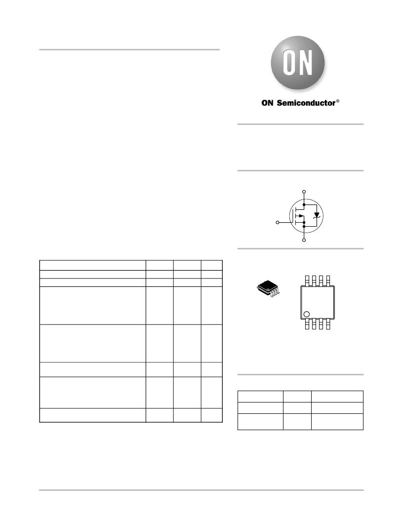 �
�
�NTTD1P02R2�
�Power� MOSFET�
�?1.45� Amps,� ?20� Volts�
�P� ?� Channel� Enhancement� Mode�
�Dual� Micro8� t� Package�
�Features�
�?� Ultra� Low� R� DS(on)�
�?� Higher� Efficiency� Extending� Battery� Life�
�?� Logic� Level� Gate� Drive�
�?� Miniature� Dual� Micro8� Surface� Mount� Package�
�?� Diode� Exhibits� High� Speed,� Soft� Recovery�
�?� Micro8� Mounting� Information� Provided�
�?� Pb� ?� Free� Package� is� Available�
�Applications�
�?� Power� Management� in� Portable� and� Battery� ?� Powered� Products,�
�i.e.:� Computers,� Printers,� PCMCIA� Cards,� Cellular� and� Cordless�
�Telephones�
�MAXIMUM� RATINGS� (T� J� =� 25� °� C� unless� otherwise� noted)�
�http://onsemi.com�
�?� 1.45� AMPERES�
�?� 20� VOLTS�
�160� m� W� @� V� GS� =� ?� 4.5�
�Dual� P� ?� Channel�
�D�
�G�
�S�
�MARKING� DIAGRAM� &�
�Rating�
�Drain� ?� to� ?� Source� Voltage�
�Gate� ?� to� ?� Source� Voltage� ?� Continuous�
�Thermal� Resistance� ?�
�Junction� ?� to� ?� Ambient� (Note� 1)�
�Total� Power� Dissipation� @� T� A� =� 25� °� C�
�Continuous� Drain� Current� @� T� A� =� 25� °� C�
�Continuous� Drain� Current� @� T� A� =� 70� °� C�
�Pulsed� Drain� Current� (Note� 3)�
�Thermal� Resistance� ?�
�Junction� ?� to� ?� Ambient� (Note� 2)�
�Total� Power� Dissipation� @� T� A� =� 25� °� C�
�Continuous� Drain� Current� @� T� A� =� 25� °� C�
�Continuous� Drain� Current� @� T� A� =� 70� °� C�
�Pulsed� Drain� Current� (Note� 3)�
�Symbol�
�V� DSS�
�V� GS�
�R� q� JA�
�P� D�
�I� D�
�I� D�
�I� DM�
�R� q� JA�
�P� D�
�I� D�
�I� D�
�I� DM�
�Value�
�?� 20�
�"� 8.0�
�250�
�0.50�
�?� 1.45�
�?� 1.15�
�?� 10�
�125�
�1.0�
�?� 2.04�
�?� 1.64�
�?� 16�
�Unit�
�V�
�V�
�°� C/W�
�W�
�A�
�A�
�A�
�°� C/W�
�W�
�A�
�A�
�A�
�8�
�1�
�Micro8�
�CASE� 846A�
�STYLE� 2�
�BC�
�WW�
�G�
�PIN� ASSIGNMENT�
�D1� D1� D2� D2�
�8�
�WW�
�BC� G�
�G�
�1�
�S1� G1� S2� G2�
�=� Specific� Device� Code�
�=� Work� Week�
�=� Pb� ?� Free� Package�
�Operating� and� Storage�
�Temperature� Range�
�Single� Pulse� Drain� ?� to� ?� Source� Avalanche�
�Energy� ?� Starting� T� J� =� 25� °� C�
�(V� DD� =� ?� 20� Vdc,� V� GS� =� ?� 4.5� Vdc,�
�Peak� I� L� =� ?� 3.5� Apk,� L� =� 5.6� mH,�
�R� G� =� 25� W� )�
�Maximum� Lead� Temperature� for� Soldering�
�Purposes� for� 10� seconds�
�T� J� ,� T� stg�
�EAS�
�T� L�
�?� 55� to�
�+150�
�35�
�260�
�°� C�
�mJ�
�°� C�
�(Note:� Microdot� may� be� in� either� location)�
�ORDERING� INFORMATION�
�Device� Package� Shipping� ?�
�NTTD1P02R2� Micro8� 4000/Tape� &� Reel�
�NTTD1P02R2G� Micro8� 4000/Tape� &� Reel�
�Stresses� exceeding� Maximum� Ratings� may� damage� the� device.� Maximum�
�Ratings� are� stress� ratings� only.� Functional� operation� above� the� Recommended�
�Operating� Conditions� is� not� implied.� Extended� exposure� to� stresses� above� the�
�Recommended� Operating� Conditions� may� affect� device� reliability.�
�1.� Minimum� FR� ?� 4� or� G� ?� 10� PCB,� Steady� State.�
�2.� Mounted� onto� a� 2”� square� FR� ?� 4� Board�
�(1� in� sq,� 2� oz� Cu� 0.06� ″� thick� single� sided),� Steady� State.�
�3.� Pulse� Test:� Pulse� Width� =� 300� m� s,� Duty� Cycle� =� 2%.�
�(Pb� ?� Free)�
�?For� information� on� tape� and� reel� specifications,�
�including� part� orientation� and� tape� sizes,� please�
�refer� to� our� Tape� and� Reel� Packaging� Specification�
�Brochure,� BRD8011/D.�
�?� Semiconductor� Components� Industries,� LLC,� 2006�
�March,� 2006� ?� Rev.� 2�
�1�
�Publication� Order� Number:�
�NTTD1P02R2/D�
�相关PDF资料 |
PDF描述 |
|---|---|
| NTTD4401FR2 | MOSFET P-CH 20V 2.4A 8MICRO |
| NTTFS4800NTAG | MOSFET N-CH 30V 5A 8WDFN |
| NTTFS4821NTAG | MOSFET N-CH 30V 7.5A 8WDFN |
| NTTFS4823NTWG | MOSFET N-CH 30V 7.1A 8WDFN |
| NTTFS4824NTWG | MOSFET N-CH 30V 8.3A 8WDFN |
相关代理商/技术参数 |
参数描述 |
|---|---|
| NTTD2P02R2 | 制造商:未知厂家 制造商全称:未知厂家 功能描述:TRANSISTOR | MOSFET | MATCHED PAIR | P-CHANNEL | 20V V(BR)DSS | 2.4A I(D) | TSSOP |
| NTTD2P02R2/D | 制造商:未知厂家 制造商全称:未知厂家 功能描述:Power MOSFET -2.4 Amps, -20 Volts |
| NTTD4401F | 制造商:ONSEMI 制造商全称:ON Semiconductor 功能描述:Power MOSFET and Schottky Diode |
| NTTD4401F_07 | 制造商:ONSEMI 制造商全称:ON Semiconductor 功能描述:Power MOSFET and Schottky Diode |
| NTTD4401FR2 | 功能描述:MOSFET -20V -3.3A P-Channel RoHS:否 制造商:STMicroelectronics 晶体管极性:N-Channel 汲极/源极击穿电压:650 V 闸/源击穿电压:25 V 漏极连续电流:130 A 电阻汲极/源极 RDS(导通):0.014 Ohms 配置:Single 最大工作温度: 安装风格:Through Hole 封装 / 箱体:Max247 封装:Tube |
发布紧急采购,3分钟左右您将得到回复。