- 您现在的位置:买卖IC网 > Datasheet目录493 > NTY100N10G (ON Semiconductor)MOSFET N-CH 100V 123A TO-264 Datasheet资料下载
参数资料
| 型号: | NTY100N10G |
| 厂商: | ON Semiconductor |
| 文件页数: | 1/8页 |
| 文件大小: | 0K |
| 描述: | MOSFET N-CH 100V 123A TO-264 |
| 产品变化通告: | Product Obsolescence 01/Jul/2009 |
| 标准包装: | 25 |
| FET 型: | MOSFET N 通道,金属氧化物 |
| FET 特点: | 标准 |
| 漏极至源极电压(Vdss): | 100V |
| 电流 - 连续漏极(Id) @ 25° C: | 123A |
| 开态Rds(最大)@ Id, Vgs @ 25° C: | 10 毫欧 @ 50A,10V |
| Id 时的 Vgs(th)(最大): | 4V @ 250µA |
| 闸电荷(Qg) @ Vgs: | 350nC @ 10V |
| 输入电容 (Ciss) @ Vds: | 10110pF @ 25V |
| 功率 - 最大: | 313W |
| 安装类型: | 通孔 |
| 封装/外壳: | TO-264-3,TO-264AA |
| 供应商设备封装: | TO-264 |
| 包装: | 管件 |
�� �
�
�NTY100N10�
�Preferred� Device�
�Power� MOSFET� 123� A,�
�100� V� N?Channel�
�Enhancement?Mode� TO264�
�Package�
�http://onsemi.com�
�Features�
�?� Source� ?� to� ?� Drain� Diode� Recovery� Time� Comparable� to� a� Discrete�
�Fast� Recovery� Diode�
�?� Avalanche� Energy� Specified�
�?� IDSS� and� R� DS(on)� Specified� at� Elevated� Temperature�
�?� Pb� ?� Free� Package� is� Available*�
�Applications�
�?� PWM� Motor� Control�
�?� Power� Supplies�
�?� Converters�
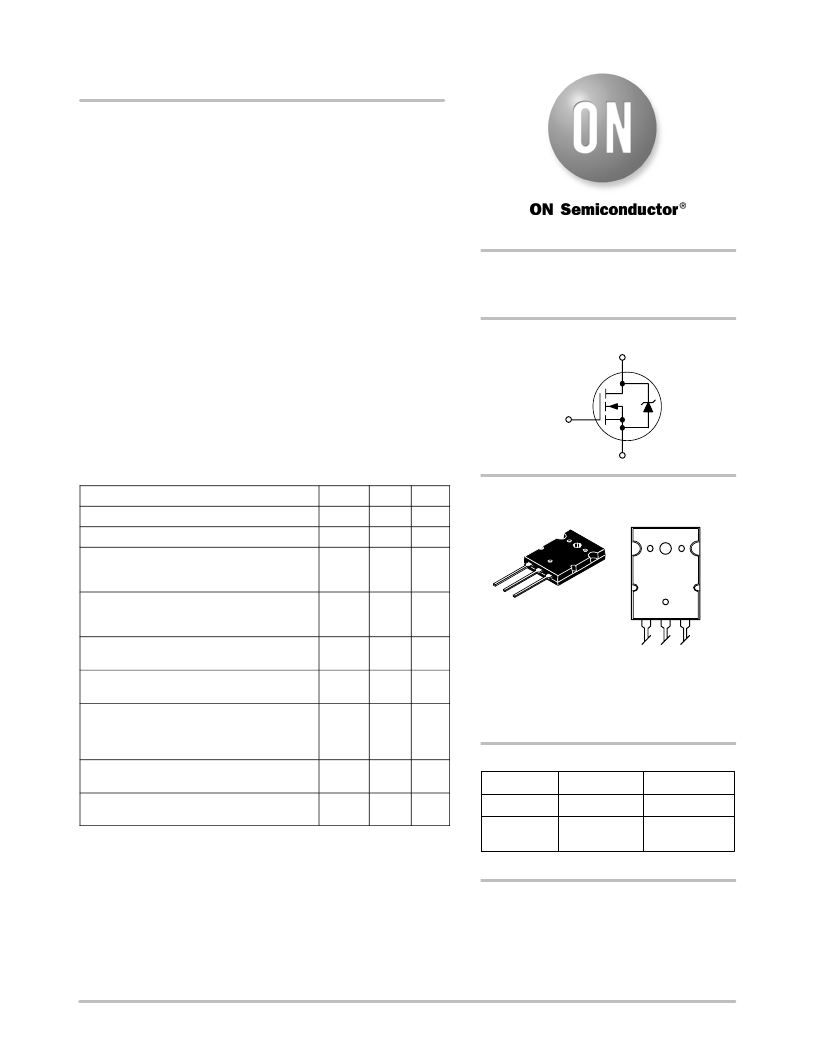
�123� A,� 100� V�
�9� m� W� @� V� GS� =� 10� V� (Typ)�
�N� ?� Channel�
�D�
�G�
�S�
�MAXIMUM� RATINGS� (T� C� =� 25� °� C� unless� otherwise� noted)�
�Rating�
�Drain� ?� Source� Voltage�
�Drain� ?� Gate� Voltage� (R� GS� =� 1� M� W� )�
�Symbol�
�V� DSS�
�V� DGR�
�Value�
�100�
�100�
�Unit�
�V�
�V�
�MARKING� DIAGRAM� &�
�PIN� ASSIGNMENT�
�Gate� ?� Source� Voltage�
�?� Continuous�
�?� Non� ?� Repetitive� (t� p� v� 10� ms)�
�Drain� Current� (Note� 1)�
�?� Continuous� @� T� C� =� 25� °� C�
�?� Pulsed�
�Total� Power� Dissipation� (Note� 1)�
�Derate� above� 25� °� C�
�V� GS�
�V� GSM�
�I� D�
�I� DM�
�P� D�
�$� 20�
�$� 40�
�123�
�369�
�313�
�2.5�
�V�
�V�
�A�
�A�
�Watts�
�W/� °� C�
�1�
�2�
�3�
�TO� ?� 264�
�CASE� 340G�
�STYLE� 1�
�NTY100N10�
�AYYWWG�
�1� 2� 3�
�G� D� S�
�Operating� and� Storage� Temperature� Range�
�T� J� ,� T� stg�
�?� 55� to�
�150�
�°� C�
�A�
�YY�
�=� Assembly� Location�
�=� Year�
�Single� Pulse� Drain� ?� to� ?� Source�
�Avalanche� Energy� ?� Starting� T� J� =� 25� °� C�
�(V� DD� =� 80� Vdc,� V� GS� =� 10� Vdc,�
�Peak� I� L� =� 100� Apk,� L� =� 0.1� mH,� R� G� =� 25� W� )�
�Thermal� Resistance� ?� Junction� to� Case�
�?� Junction� to� Ambient�
�E� AS�
�R� q� JC�
�R� q� JA�
�500�
�0.4�
�25�
�mJ�
�°� C/W�
�WW� =� Work� Week�
�G� =� Pb� ?� Free� Package�
�ORDERING� INFORMATION�
�Device� Package� Shipping�
�Maximum� Lead� Temperature� for� Soldering�
�Purposes,� 0.125� in� from� case� for� 10� seconds�
�T� L�
�260�
�°� C�
�NTY100N10�
�NTY100N10G�
�TO� ?� 264�
�TO� ?� 264�
�25� Units/Rail�
�25� Units/Rail�
�Stresses� exceeding� Maximum� Ratings� may� damage� the� device.� Maximum�
�Ratings� are� stress� ratings� only.� Functional� operation� above� the� Recommended�
�Operating� Conditions� is� not� implied.� Extended� exposure� to� stresses� above� the�
�Recommended� Operating� Conditions� may� affect� device� reliability.�
�1.� Pulse� Test:� Pulse� Width� =� 10� m� s,� Duty� ?� Cycle� =� 2%.�
�(Pb� ?� Free)�
�Preferred� devices� are� recommended� choices� for� future� use�
�and� best� overall� value.�
�*For� additional� information� on� our� Pb� ?� Free� strategy� and� soldering� details,� please�
�download� the� ON� Semiconductor� Soldering� and� Mounting� Techniques� Reference�
�Manual,� SOLDERRM/D.�
�?� Semiconductor� Components� Industries,� LLC,� 2006�
�March,� 2006� ?� Rev.� 2�
�1�
�Publication� Order� Number:�
�NTY100N10/D�
�相关PDF资料 |
PDF描述 |
|---|---|
| NTZD3152PT5G | MOSFET P-CHAN DUAL 20V SOT-563 |
| NTZD3154NT5G | MOSFET N-CHAN DUAL 20V SOT-563 |
| NTZD3155CT2G | MOSFET N/P-CH COMPL 20V SOT-563 |
| NTZD3156CT5G | MOSFET N/P-CH 20V SOT-563 |
| NTZD5110NT5G | MOSFET N-CH DUAL 60V SOT563 |
相关代理商/技术参数 |
参数描述 |
|---|---|
| NTZA3DVV2 | 制造商:Omron Corporation 功能描述: |
| NTZD3151P | 制造商:ONSEMI 制造商全称:ON Semiconductor 功能描述:High Efficiency DC-DC Converters |
| NTZD3152P | 制造商:ONSEMI 制造商全称:ON Semiconductor 功能描述:Small Signal MOSFET −20 V, −430 mA, Dual P−Channel with ESD Protection, SOT−563 |
| NTZD3152PT1G | 功能描述:MOSFET -20V -430mA Dual P-Channel RoHS:否 制造商:STMicroelectronics 晶体管极性:N-Channel 汲极/源极击穿电压:650 V 闸/源击穿电压:25 V 漏极连续电流:130 A 电阻汲极/源极 RDS(导通):0.014 Ohms 配置:Single 最大工作温度: 安装风格:Through Hole 封装 / 箱体:Max247 封装:Tube |
| NTZD3152PT1H | 制造商:ON Semiconductor 功能描述:PFET SOT563 20V 430MA 900 - Tape and Reel 制造商:ON Semiconductor 功能描述:PFET SOT563 20V 430MA TR 制造商:Rochester Electronics LLC 功能描述: 制造商:ON Semiconductor 功能描述:REEL / PFET SOT563 20V 430MA TR |
发布紧急采购,3分钟左右您将得到回复。