- 您现在的位置:买卖IC网 > Datasheet目录495 > OP573 (TT Electronics/Optek Technology)PHOTOTRANSISTOR NPN SND REV GULL Datasheet资料下载
参数资料
| 型号: | OP573 |
| 厂商: | TT Electronics/Optek Technology |
| 文件页数: | 3/4页 |
| 文件大小: | 0K |
| 描述: | PHOTOTRANSISTOR NPN SND REV GULL |
| 标准包装: | 1 |
| 系列: | * |
| 电压 - 集电极发射极击穿(最大): | 30V |
| 电流 - 集电极 (Ic)(最大): | 20mA |
| 电流 - 暗 (Id)(最大): | 100nA |
| 波长: | 935nm |
| 视角: | 25° |
| 功率 - 最大: | 130mW |
| 安装类型: | 表面贴装 |
| 方向: | 顶视图 |
| 封装/外壳: | 2-SMD,Z形弯曲d |
| 其它名称: | 365-1161-6 |
�� �
�
�Silicon� Phototransistor�
�OP570� Series�
�Absolute� Maximum� Ratings� (T� A� =25°C� unless� otherwise� noted)�
�Storage� Temperature� Range�
�Operating� Temperature� Range�
�Collector-Emitter� Voltage�
�Emitter-Collector� Voltage�
�Collector� Current�
�Lead� Soldering� Temperature� [1/16� inch� (1.6� mm)� from� case� for� 5� seconds� with� soldering� iron]�
�Power� Dissipation�
�Notes:�
�1.� Solder� time� less� than� 5� seconds� at� temperature� extreme.�
�2.� Derate� linearly� at� 2.17� mW/°� C� above� 25°� C.�
�Electrical� Characteristics� (T� A� =� 25� °� C� unless� otherwise� noted)�
�-40� o� C� to� +85� o� C�
�-25� o� C� to� +85� o� C�
�30� V�
�5V�
�20� mA�
�260°� C� (1)�
�130� mW� (2)�
�SYMBOL�
�PARAMETER�
�MIN�
�TYP�
�MAX�
�UNITS�
�TEST� CONDITIONS�
�Input� Diode�
�I� C� (ON)�
�On-State� Collector� Current�
�2.5�
�-�
�-�
�mA�
�V� CE� =� 5.0� V,� E� E� =� 5.0� mW/cm� 2�
�(1)�
�V� CE(SAT)�
�I� CEO�
�V� BR(CEO)�
�V� (BR)ECO�
�Forward� Voltage�
�Reverse� Current�
�Wavelength� at� Peak� Emission�
�Emission� Angle� at� Half� Power� Points�
�-�
�-�
�30�
�5�
�-�
�-�
�-�
�-�
�0.4�
�100�
�-�
�-�
�V�
�nA�
�V�
�V�
�I� C� =� 100� μA,� E� E� =� 2.0� mW/cm� 2� (1)�
�V� CE� =� 5.0� V,� E� E� =� 0� (2)�
�I� C� =� 100� μA�
�I� E� =� 100� μA�
�Notes:�
�1.� Light� source� is� an� unfiltered� GaAl� LED� with� a� peak� emission� wavelength� of� 935nm� and� a� radiometric� intensity� level� which� varies� less�
�than� 10%� over� the� entire� lens� surface� of� the� phototransistor� being� tested.�
�2.� To� calculate� typical� collector� dark� current� in� μA,� use� the� formula� I� CEO� =� 10�
�(0.04� Ta-3.4)�
�where� Ta� is� the� ambient� temperature� in� °� C.�
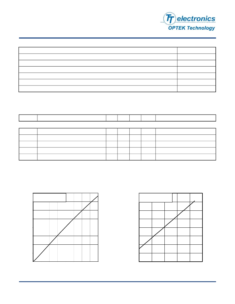
�Relative� On-State� Collector�
�Relative� On-State� Collector� Current�
�160%�
�140%�
�120%�
�100%�
�80%�
�60%�
�40%�
�20%�
�Current� vs.� Irradiance�
�Normalized� at� E� e� =� 5mW/cm� 2�
�Conditions:� V� CE� =� 5V,�
�λ� =� 935nm,� T� A� =� 25� °C�
�140%�
�130%�
�120%�
�110%�
�100%�
�90%�
�80%�
�70%�
�vs.� Temperature�
�Normalized� at� T� A� =� 25°C� .�
�Conditions:� V� CE� =� 5V,�
�λ� =� 935nm,� T� A� =� 25� °C�
�0�
�1.0�
�2.0�
�3.0�
�4.0�
�5.0�
�6.0�
�7.0�
�8.0�
�-25�
�0�
�25�
�50�
�75�
�100�
�Ee—Irradiance� (mW/cm� )�
�2�
�Temperature—(°C)�
�OPTEK� reserves� the� right� to� make� changes� at� any� time� in� order� to� improve� design� and� to� supply� the� best� product� possible.�
�OPTEK� Technology� Inc.� —� 1645� Wallace� Drive,� Carrollton,� Texas� 75006�
�Phone:� (972)� 323-2200� or� (800)� 341-4747� FAX:� (972)� 323-2396� sensors@optekinc.com� www.optekinc.com�
�Issue� 1.2� 02/07�
�Page� 3� of� 4�
�相关PDF资料 |
PDF描述 |
|---|---|
| OP580DA | PHOTODARLINGTON NPN CLR PLCC-2 |
| OP580 | PHOTOTRANSISTOR NPN SMD PLCC-2 |
| OP598C | PHOTOTRNS PLSTIC SILCN NPN T13/4 |
| OP599C | PHOTOTRNS PLSTIC SILCN NPN T13/4 |
| OP600B | PHOTOTRNS SILCN NPN HERMETC PILL |
相关代理商/技术参数 |
参数描述 |
|---|---|
| OP578/A,025 | 功能描述:MOSFET OP578/UNCASED/JAR//A RoHS:否 制造商:STMicroelectronics 晶体管极性:N-Channel 汲极/源极击穿电压:650 V 闸/源击穿电压:25 V 漏极连续电流:130 A 电阻汲极/源极 RDS(导通):0.014 Ohms 配置:Single 最大工作温度: 安装风格:Through Hole 封装 / 箱体:Max247 封装:Tube |
| OP579/A,025 | 功能描述:MOSFET OP579/UNCASED/JAR//A RoHS:否 制造商:STMicroelectronics 晶体管极性:N-Channel 汲极/源极击穿电压:650 V 闸/源击穿电压:25 V 漏极连续电流:130 A 电阻汲极/源极 RDS(导通):0.014 Ohms 配置:Single 最大工作温度: 安装风格:Through Hole 封装 / 箱体:Max247 封装:Tube |
| OP580 | 功能描述:光电晶体管 Phototransistor RoHS:否 制造商:OSRAM Opto Semiconductors 最大功率耗散:165 mW 最大暗电流:200 nA 封装 / 箱体:T-1 |
| OP580 | 制造商:TT Electronics / OPTEK Technology 功能描述:Phototransistor |
| OP580/ABD,029 | 功能描述:MOSFET OP580/UNCASED/PUTA// RoHS:否 制造商:STMicroelectronics 晶体管极性:N-Channel 汲极/源极击穿电压:650 V 闸/源击穿电压:25 V 漏极连续电流:130 A 电阻汲极/源极 RDS(导通):0.014 Ohms 配置:Single 最大工作温度: 安装风格:Through Hole 封装 / 箱体:Max247 封装:Tube |
发布紧急采购,3分钟左右您将得到回复。