- 您现在的位置:买卖IC网 > PDF目录189414 > OR2T10A-4S352 (Electronic Theatre Controls, Inc.) Field-Programmable Gate Arrays PDF资料下载
参数资料
| 型号: | OR2T10A-4S352 |
| 厂商: | Electronic Theatre Controls, Inc. |
| 元件分类: | FPGA |
| 英文描述: | Field-Programmable Gate Arrays |
| 中文描述: | 现场可编程门阵列 |
| 文件页数: | 118/192页 |
| 文件大小: | 3148K |
| 代理商: | OR2T10A-4S352 |
第1页第2页第3页第4页第5页第6页第7页第8页第9页第10页第11页第12页第13页第14页第15页第16页第17页第18页第19页第20页第21页第22页第23页第24页第25页第26页第27页第28页第29页第30页第31页第32页第33页第34页第35页第36页第37页第38页第39页第40页第41页第42页第43页第44页第45页第46页第47页第48页第49页第50页第51页第52页第53页第54页第55页第56页第57页第58页第59页第60页第61页第62页第63页第64页第65页第66页第67页第68页第69页第70页第71页第72页第73页第74页第75页第76页第77页第78页第79页第80页第81页第82页第83页第84页第85页第86页第87页第88页第89页第90页第91页第92页第93页第94页第95页第96页第97页第98页第99页第100页第101页第102页第103页第104页第105页第106页第107页第108页第109页第110页第111页第112页第113页第114页第115页第116页第117页当前第118页第119页第120页第121页第122页第123页第124页第125页第126页第127页第128页第129页第130页第131页第132页第133页第134页第135页第136页第137页第138页第139页第140页第141页第142页第143页第144页第145页第146页第147页第148页第149页第150页第151页第152页第153页第154页第155页第156页第157页第158页第159页第160页第161页第162页第163页第164页第165页第166页第167页第168页第169页第170页第171页第172页第173页第174页第175页第176页第177页第178页第179页第180页第181页第182页第183页第184页第185页第186页第187页第188页第189页第190页第191页第192页
Data Sheet
June 1999
ORCA Series 2 FPGAs
Lucent Technologies Inc.
31
Programmable Input/Output Cells
(continued)
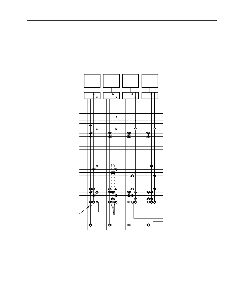
Figure 27 shows paths to and from pads and the use of MUX CIPs to connect lines. Detail A shows six MUX CIPs
for the pad P0 used to construct the net for the 3-state signal. In the MUX CIP, one of six lines is connected to a line
to form the net. In this case, the ts0 signal can be driven by either of the two PXLs, PX1[0], PX1[1], XSW[0], or the
LLDRV lines. Detail B shows the four MUX CIPs used to drive the P1 output. The source line for OUT1 is either
XSW[1], PX1[1], PX1[3], or PX2[2].
5-2843.BL(F).2C.r3
Figure 27. PIC Detail
DT
PA
PB
PC
PD
TS
0
OUT0
IN0
DOUT0
TS
1
OUT1
IN1
DOUT1
TS
3
OUT3
IN3
DOUT3
TS
2
OUT2
IN2
DOUT2
PXL[1]
PXL[0]
PX2[2]
PX2[3]
PX2[0]
PX2[1]
PX1[0]
PX1[1]
PX1[2]
PX1[3]
PXH[1]
PXH[2]
PXH[3]
PXH[0]
PXL[1]
PXL[0]
PX2[2]
PX2[3]
PX2[0]
PX2[1]
PX1[0]
PX1[1]
PX1[2]
PX1[3]
PXH[1]
PXH[2]
PXH[3]
PXH[0]
DOUT[0]
DOUT[1]
DOUT[2]
DOUT[3]
XSW[0]
XSW[1]
XSW[2]
XSW[3]
LLDRV
A
B
相关PDF资料 |
PDF描述 |
|---|---|
| OR2T10A-4S256I | Field-Programmable Gate Arrays |
| OR2T10A-4S256 | Field-Programmable Gate Arrays |
| OR2T10A-4S240I | Field-Programmable Gate Arrays |
| OR2T10A-4S240 | Field-Programmable Gate Arrays |
| OR2T10A-4S208I | Field-Programmable Gate Arrays |
相关代理商/技术参数 |
参数描述 |
|---|---|
| OR2T10A5BA256-DB | 功能描述:FPGA - 现场可编程门阵列 1024 LUT 244 I/O RoHS:否 制造商:Altera Corporation 系列:Cyclone V E 栅极数量: 逻辑块数量:943 内嵌式块RAM - EBR:1956 kbit 输入/输出端数量:128 最大工作频率:800 MHz 工作电源电压:1.1 V 最大工作温度:+ 70 C 安装风格:SMD/SMT 封装 / 箱体:FBGA-256 |
| OR2T10A5J160-DB | 功能描述:FPGA - 现场可编程门阵列 1024 LUT 244 I/O RoHS:否 制造商:Altera Corporation 系列:Cyclone V E 栅极数量: 逻辑块数量:943 内嵌式块RAM - EBR:1956 kbit 输入/输出端数量:128 最大工作频率:800 MHz 工作电源电压:1.1 V 最大工作温度:+ 70 C 安装风格:SMD/SMT 封装 / 箱体:FBGA-256 |
| OR2T10A5S208-DB | 功能描述:FPGA - 现场可编程门阵列 1024 LUT 244 I/O RoHS:否 制造商:Altera Corporation 系列:Cyclone V E 栅极数量: 逻辑块数量:943 内嵌式块RAM - EBR:1956 kbit 输入/输出端数量:128 最大工作频率:800 MHz 工作电源电压:1.1 V 最大工作温度:+ 70 C 安装风格:SMD/SMT 封装 / 箱体:FBGA-256 |
| OR2T10A5S240-DB | 功能描述:FPGA - 现场可编程门阵列 Use ECP/EC or XP RoHS:否 制造商:Altera Corporation 系列:Cyclone V E 栅极数量: 逻辑块数量:943 内嵌式块RAM - EBR:1956 kbit 输入/输出端数量:128 最大工作频率:800 MHz 工作电源电压:1.1 V 最大工作温度:+ 70 C 安装风格:SMD/SMT 封装 / 箱体:FBGA-256 |
| OR2T12A4BA256-DB | 制造商:Rochester Electronics LLC 功能描述:- Bulk 制造商:Lattice Semiconductor Corporation 功能描述: |
发布紧急采购,3分钟左右您将得到回复。