- 您现在的位置:买卖IC网 > PDF目录189414 > OR2T10A-4S352 (Electronic Theatre Controls, Inc.) Field-Programmable Gate Arrays PDF资料下载
参数资料
| 型号: | OR2T10A-4S352 |
| 厂商: | Electronic Theatre Controls, Inc. |
| 元件分类: | FPGA |
| 英文描述: | Field-Programmable Gate Arrays |
| 中文描述: | 现场可编程门阵列 |
| 文件页数: | 57/192页 |
| 文件大小: | 3148K |
| 代理商: | OR2T10A-4S352 |
第1页第2页第3页第4页第5页第6页第7页第8页第9页第10页第11页第12页第13页第14页第15页第16页第17页第18页第19页第20页第21页第22页第23页第24页第25页第26页第27页第28页第29页第30页第31页第32页第33页第34页第35页第36页第37页第38页第39页第40页第41页第42页第43页第44页第45页第46页第47页第48页第49页第50页第51页第52页第53页第54页第55页第56页当前第57页第58页第59页第60页第61页第62页第63页第64页第65页第66页第67页第68页第69页第70页第71页第72页第73页第74页第75页第76页第77页第78页第79页第80页第81页第82页第83页第84页第85页第86页第87页第88页第89页第90页第91页第92页第93页第94页第95页第96页第97页第98页第99页第100页第101页第102页第103页第104页第105页第106页第107页第108页第109页第110页第111页第112页第113页第114页第115页第116页第117页第118页第119页第120页第121页第122页第123页第124页第125页第126页第127页第128页第129页第130页第131页第132页第133页第134页第135页第136页第137页第138页第139页第140页第141页第142页第143页第144页第145页第146页第147页第148页第149页第150页第151页第152页第153页第154页第155页第156页第157页第158页第159页第160页第161页第162页第163页第164页第165页第166页第167页第168页第169页第170页第171页第172页第173页第174页第175页第176页第177页第178页第179页第180页第181页第182页第183页第184页第185页第186页第187页第188页第189页第190页第191页第192页
Lucent Technologies Inc.
15
Data Sheet
June 1999
ORCA Series 2 FPGAs
Programmable Logic Cells (continued)
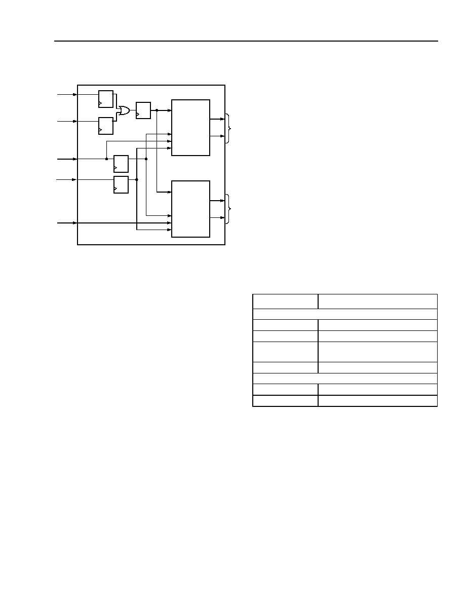
5-4641(F).r1
Figure 17. SDPM Mode—16 x 2 Synchronous
Dual-Port Memory
The Series 2 devices have added a second synchro-
nous memory mode known as the synchronous dual-
port memory (SDPM) mode. This mode writes data
into the memory synchronously in the same manner
described previously for SSPM mode. The SDPM
mode differs in that two separate 16 x 2 memories are
created in each PFU that have the same WE, WPE,
write data (WD[1:0]), and write address (WA[3:0])
inputs, as shown in Figure 17.
The outputs of HLUTA (F[3:2]) operate the same way
they do in SSPM mode—the read address comes
directly from the A[3:0] inputs used to create the
latched write address. The outputs of HLUTB (F[1:0])
operate in a dual-port mode where the write address
comes from the latched version of A[3:0], and the read
address comes directly from RA[3:0], which is input on
B[3:0].
Since external multiplexing of the write address and
read address is not required, extremely fast RAMs can
be created. New system applications that require an
interface between two different asynchronous clocks
can also be implemented using the SDPM mode. An
example of this is accomplished by creating FIFOs
where one clock controls the synchronous write of data
into the FIFO, and the other clock controls the read
address to allow reading of data at any time from the
FIFO.
Latches/Flip-Flops
The four latches/FFs in the PFU can be used in a vari-
ety of configurations. In some cases, the configuration
options apply to all four latches/FFs in the PFU. For
other options, each latch/FF is independently program-
mable.
Table 4 summarizes these latch/FF options. The
latches/FFs can be configured as either positive or
negative level-sensitive latches, or positive or negative
edge-triggered flip-flops. All latches/FFs in a given PFU
share the same clock, and the clock to these latches/
FFs can be inverted. The input into each latch/FF is
from either the corresponding QLUT output (F[3:0]) or
the direct data input (WD[3:0]). For latches/FFs located
in the two outer rings of PLCs, additional inputs are
possible. These additional inputs are fast paths from
I/O pads located in PICs in the same row or column as
the PLCs. If the latch/FF is not located in the two outer
rings of the PLCs, the latch/FF input can also be tied to
logic 0, which is the default. The four latch/FF outputs,
Q[3:0], can be placed on the five PFU outputs, O[4:0].
Table 4. Configuration RAM Controlled Latch/
Flip-Flop Operation
The four latches/FFs in a PFU share the clock (CK),
clock enable (CE), and local set/reset (LSR) inputs.
When CE is disabled, each latch/FF retains its previous
value when clocked. Both the clock enable and LSR
inputs can be inverted to be active-low.
WE
WPE
A4
DQ
CIN, C0
WA[3:0]
WD[1:0]
WR
WA[3:0]
RA[3:0]
WD[1:0]
HLUTA
F3
F2
DQ
WR
WA[3:0]
RA[3:0]
WD[1:0]
HLUTB
F1
F0
WRITE PULSE
GENERATOR
A[3:0]
WD[1:0]
RA[3:0] B[3:0]
SS
PM
OUTPU
T
SD
P
M
O
U
TP
U
T
Function
Options
Functionality Common to All Latch/FFs in PFU
LSR Operation
Asynchronous or synchronous
Clock Polarity
Noninverted or inverted
Front-End Select
Direct (WD[3:0]) or from LUT
(F[3:0])
LSR Priority
Either LSR or CE has priority
Functionality Set Individually in Each Latch/FF in PFU
Latch/FF Mode
Latch or flip-flop
Set/Reset Mode
Set or Reset
相关PDF资料 |
PDF描述 |
|---|---|
| OR2T10A-4S256I | Field-Programmable Gate Arrays |
| OR2T10A-4S256 | Field-Programmable Gate Arrays |
| OR2T10A-4S240I | Field-Programmable Gate Arrays |
| OR2T10A-4S240 | Field-Programmable Gate Arrays |
| OR2T10A-4S208I | Field-Programmable Gate Arrays |
相关代理商/技术参数 |
参数描述 |
|---|---|
| OR2T10A5BA256-DB | 功能描述:FPGA - 现场可编程门阵列 1024 LUT 244 I/O RoHS:否 制造商:Altera Corporation 系列:Cyclone V E 栅极数量: 逻辑块数量:943 内嵌式块RAM - EBR:1956 kbit 输入/输出端数量:128 最大工作频率:800 MHz 工作电源电压:1.1 V 最大工作温度:+ 70 C 安装风格:SMD/SMT 封装 / 箱体:FBGA-256 |
| OR2T10A5J160-DB | 功能描述:FPGA - 现场可编程门阵列 1024 LUT 244 I/O RoHS:否 制造商:Altera Corporation 系列:Cyclone V E 栅极数量: 逻辑块数量:943 内嵌式块RAM - EBR:1956 kbit 输入/输出端数量:128 最大工作频率:800 MHz 工作电源电压:1.1 V 最大工作温度:+ 70 C 安装风格:SMD/SMT 封装 / 箱体:FBGA-256 |
| OR2T10A5S208-DB | 功能描述:FPGA - 现场可编程门阵列 1024 LUT 244 I/O RoHS:否 制造商:Altera Corporation 系列:Cyclone V E 栅极数量: 逻辑块数量:943 内嵌式块RAM - EBR:1956 kbit 输入/输出端数量:128 最大工作频率:800 MHz 工作电源电压:1.1 V 最大工作温度:+ 70 C 安装风格:SMD/SMT 封装 / 箱体:FBGA-256 |
| OR2T10A5S240-DB | 功能描述:FPGA - 现场可编程门阵列 Use ECP/EC or XP RoHS:否 制造商:Altera Corporation 系列:Cyclone V E 栅极数量: 逻辑块数量:943 内嵌式块RAM - EBR:1956 kbit 输入/输出端数量:128 最大工作频率:800 MHz 工作电源电压:1.1 V 最大工作温度:+ 70 C 安装风格:SMD/SMT 封装 / 箱体:FBGA-256 |
| OR2T12A4BA256-DB | 制造商:Rochester Electronics LLC 功能描述:- Bulk 制造商:Lattice Semiconductor Corporation 功能描述: |
发布紧急采购,3分钟左右您将得到回复。