- 您现在的位置:买卖IC网 > PDF目录189414 > OR2T10A-4S352 (Electronic Theatre Controls, Inc.) Field-Programmable Gate Arrays PDF资料下载
参数资料
| 型号: | OR2T10A-4S352 |
| 厂商: | Electronic Theatre Controls, Inc. |
| 元件分类: | FPGA |
| 英文描述: | Field-Programmable Gate Arrays |
| 中文描述: | 现场可编程门阵列 |
| 文件页数: | 137/192页 |
| 文件大小: | 3148K |
| 代理商: | OR2T10A-4S352 |
第1页第2页第3页第4页第5页第6页第7页第8页第9页第10页第11页第12页第13页第14页第15页第16页第17页第18页第19页第20页第21页第22页第23页第24页第25页第26页第27页第28页第29页第30页第31页第32页第33页第34页第35页第36页第37页第38页第39页第40页第41页第42页第43页第44页第45页第46页第47页第48页第49页第50页第51页第52页第53页第54页第55页第56页第57页第58页第59页第60页第61页第62页第63页第64页第65页第66页第67页第68页第69页第70页第71页第72页第73页第74页第75页第76页第77页第78页第79页第80页第81页第82页第83页第84页第85页第86页第87页第88页第89页第90页第91页第92页第93页第94页第95页第96页第97页第98页第99页第100页第101页第102页第103页第104页第105页第106页第107页第108页第109页第110页第111页第112页第113页第114页第115页第116页第117页第118页第119页第120页第121页第122页第123页第124页第125页第126页第127页第128页第129页第130页第131页第132页第133页第134页第135页第136页当前第137页第138页第139页第140页第141页第142页第143页第144页第145页第146页第147页第148页第149页第150页第151页第152页第153页第154页第155页第156页第157页第158页第159页第160页第161页第162页第163页第164页第165页第166页第167页第168页第169页第170页第171页第172页第173页第174页第175页第176页第177页第178页第179页第180页第181页第182页第183页第184页第185页第186页第187页第188页第189页第190页第191页第192页
Lucent Technologies Inc.
49
Data Sheet
June 1999
ORCA Series 2 FPGAs
FPGA Configuration Modes (continued)
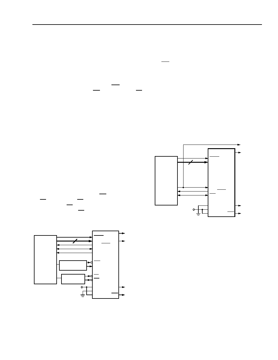
Asynchronous Peripheral Mode
Figure 42 shows the connections needed for the asyn-
chronous peripheral mode. In this mode, the FPGA
system interface is similar to that of a microprocessor-
peripheral interface. The microprocessor generates the
control signals to write an 8-bit byte into the FPGA. The
FPGA control inputs include active-low CS0 and active-
high CS1 chip selects, a write WR input, and a read RD
input. The chip selects can be cycled or maintained at
a static level during the configuration cycle. Each byte
of data is written into the FPGA’s D[7:0] input pins.
The FPGA provides a RDY status output to indicate
that another byte can be loaded. A low on RDY indi-
cates that the double-buffered hold/shift registers are
not ready to receive data, and this pin must be moni-
tored to go high before another byte of data can be
written. The shortest time RDY is low occurs when a
byte is loaded into the hold register and the shift regis-
ter is empty, in which case the byte is immediately
transferred to the shift register. The longest time for
RDY to remain low occurs when a byte is loaded into
the holding register and the shift register has just
started shifting configuration data into configuration
RAM.
The RDY status is also available on the D7 pin by
enabling the chip selects, setting WR high, and apply-
ing RD low, where the RD input is an output enable for
the D7 pin when RD is low. The D[6:0] pins are not
enabled to drive when RD is low and, thus, only act as
input pins in asynchronous peripheral mode.
5-4484(F)
Figure 42. Asynchronous Peripheral Configuration
Schematic
Synchronous Peripheral Mode
In the synchronous peripheral mode, byte-wide data is
input into D[7:0] on the rising edge of the CCLK input.
The first data byte is clocked in on the second CCLK
after INIT goes high. Subsequent data bytes are
clocked in on every eighth rising edge of CCLK. The
RDY signal is an output which acts as an acknowledge.
RDY goes high one CCLK after data is clocked and,
after one CCLK cycle, returns low. The process repeats
until all of the data is loaded into the FPGA. The data
begins shifting on DOUT 1.5 cycles after it is loaded in
parallel. It requires additional CCLKs after the last byte
is loaded to complete the shifting. Figure 43 shows the
connections for synchronous peripheral mode.
As with master modes, the peripheral modes can be
used as the lead FPGA for a daisy chain of slave
FPGAs.
5-4486(F)
Figure 43. Synchronous Peripheral Configuration
Schematic
TO DAISY-
CHAINED
DEVICES
DOUT
CCLK
HDC
LDC
VDD
ORCA
SERIES
FPGA
MICRO-
PROCESSOR
ADDRESS
DECODE LOGIC
BUS
CONTROLLER
PRGM
D[7:0]
RDY/BUSY
INIT
DONE
CS0
CS1
RD
WR
M2
M1
M0
8
TO DAISY-
CHAINED
DEVICES
DOUT
HDC
LDC
ORCA
SERIES
FPGA
MICRO-
PROCESSOR
PRGM
D[7:0]
M2
M1
M0
8
+5 V
CCLK
RDY/BUSY
INIT
相关PDF资料 |
PDF描述 |
|---|---|
| OR2T10A-4S256I | Field-Programmable Gate Arrays |
| OR2T10A-4S256 | Field-Programmable Gate Arrays |
| OR2T10A-4S240I | Field-Programmable Gate Arrays |
| OR2T10A-4S240 | Field-Programmable Gate Arrays |
| OR2T10A-4S208I | Field-Programmable Gate Arrays |
相关代理商/技术参数 |
参数描述 |
|---|---|
| OR2T10A5BA256-DB | 功能描述:FPGA - 现场可编程门阵列 1024 LUT 244 I/O RoHS:否 制造商:Altera Corporation 系列:Cyclone V E 栅极数量: 逻辑块数量:943 内嵌式块RAM - EBR:1956 kbit 输入/输出端数量:128 最大工作频率:800 MHz 工作电源电压:1.1 V 最大工作温度:+ 70 C 安装风格:SMD/SMT 封装 / 箱体:FBGA-256 |
| OR2T10A5J160-DB | 功能描述:FPGA - 现场可编程门阵列 1024 LUT 244 I/O RoHS:否 制造商:Altera Corporation 系列:Cyclone V E 栅极数量: 逻辑块数量:943 内嵌式块RAM - EBR:1956 kbit 输入/输出端数量:128 最大工作频率:800 MHz 工作电源电压:1.1 V 最大工作温度:+ 70 C 安装风格:SMD/SMT 封装 / 箱体:FBGA-256 |
| OR2T10A5S208-DB | 功能描述:FPGA - 现场可编程门阵列 1024 LUT 244 I/O RoHS:否 制造商:Altera Corporation 系列:Cyclone V E 栅极数量: 逻辑块数量:943 内嵌式块RAM - EBR:1956 kbit 输入/输出端数量:128 最大工作频率:800 MHz 工作电源电压:1.1 V 最大工作温度:+ 70 C 安装风格:SMD/SMT 封装 / 箱体:FBGA-256 |
| OR2T10A5S240-DB | 功能描述:FPGA - 现场可编程门阵列 Use ECP/EC or XP RoHS:否 制造商:Altera Corporation 系列:Cyclone V E 栅极数量: 逻辑块数量:943 内嵌式块RAM - EBR:1956 kbit 输入/输出端数量:128 最大工作频率:800 MHz 工作电源电压:1.1 V 最大工作温度:+ 70 C 安装风格:SMD/SMT 封装 / 箱体:FBGA-256 |
| OR2T12A4BA256-DB | 制造商:Rochester Electronics LLC 功能描述:- Bulk 制造商:Lattice Semiconductor Corporation 功能描述: |
发布紧急采购,3分钟左右您将得到回复。