- 您现在的位置:买卖IC网 > PDF目录189414 > OR2T10A-4S352 (Electronic Theatre Controls, Inc.) Field-Programmable Gate Arrays PDF资料下载
参数资料
| 型号: | OR2T10A-4S352 |
| 厂商: | Electronic Theatre Controls, Inc. |
| 元件分类: | FPGA |
| 英文描述: | Field-Programmable Gate Arrays |
| 中文描述: | 现场可编程门阵列 |
| 文件页数: | 24/192页 |
| 文件大小: | 3148K |
| 代理商: | OR2T10A-4S352 |
第1页第2页第3页第4页第5页第6页第7页第8页第9页第10页第11页第12页第13页第14页第15页第16页第17页第18页第19页第20页第21页第22页第23页当前第24页第25页第26页第27页第28页第29页第30页第31页第32页第33页第34页第35页第36页第37页第38页第39页第40页第41页第42页第43页第44页第45页第46页第47页第48页第49页第50页第51页第52页第53页第54页第55页第56页第57页第58页第59页第60页第61页第62页第63页第64页第65页第66页第67页第68页第69页第70页第71页第72页第73页第74页第75页第76页第77页第78页第79页第80页第81页第82页第83页第84页第85页第86页第87页第88页第89页第90页第91页第92页第93页第94页第95页第96页第97页第98页第99页第100页第101页第102页第103页第104页第105页第106页第107页第108页第109页第110页第111页第112页第113页第114页第115页第116页第117页第118页第119页第120页第121页第122页第123页第124页第125页第126页第127页第128页第129页第130页第131页第132页第133页第134页第135页第136页第137页第138页第139页第140页第141页第142页第143页第144页第145页第146页第147页第148页第149页第150页第151页第152页第153页第154页第155页第156页第157页第158页第159页第160页第161页第162页第163页第164页第165页第166页第167页第168页第169页第170页第171页第172页第173页第174页第175页第176页第177页第178页第179页第180页第181页第182页第183页第184页第185页第186页第187页第188页第189页第190页第191页第192页
12
Lucent Technologies Inc.
Data Sheet
ORCA Series 2 FPGAs
June 1999
Programmable Logic Cells (continued)
Asynchronous Memory Modes—MA and MB
The LUT in the PFU can be configured as either read/
write or read-only memory. A read/write address
(A[3:0], B[3:0]), write data (WD[1:0], WD[3:2]), and two
write-enable (WE) ports are used for memory. In asyn-
chronous memory mode, each HLUT can be used as a
16 x 2 memory. Each HLUT is configured indepen-
dently, allowing functions such as a 16 x 2 memory in
one HLUT and a logic function of five input variables or
less in the other HLUT.
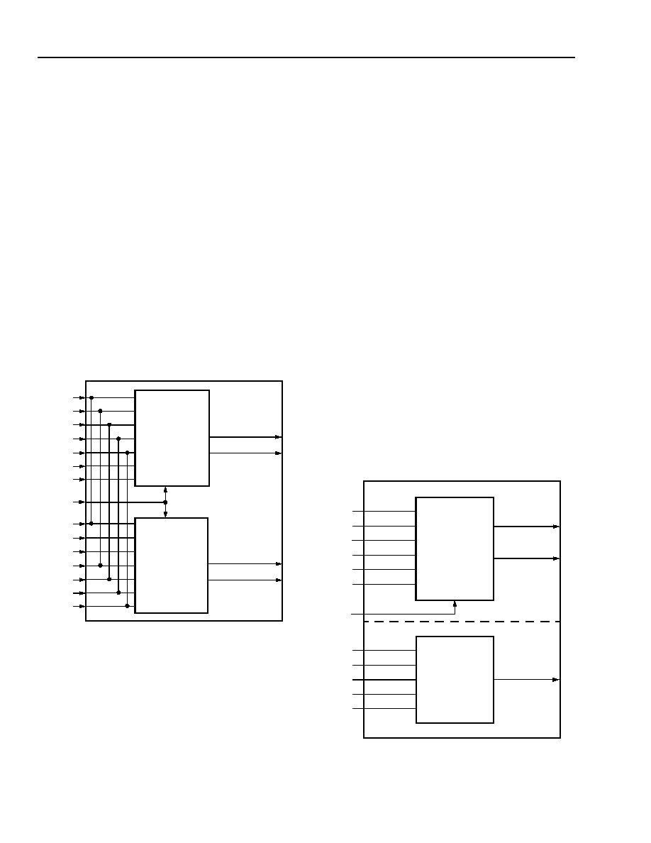
Figure 12 illustrates the use of the LUT for a 16 x 4
memory. When the LUTs are used as memory, there
are independent address, input data, and output data
buses. If the LUT is used as a 16 x 4 read/write mem-
ory, the A[3:0] and B[3:0] ports are address inputs
(A[3:0]). The A4 and B4 ports are write-enable (WE)
signals. The WD[3:0] inputs are the data inputs. The
F[3:0] data outputs can be routed out on the O[4:0]
PFU outputs or to the latch/FF D[3:0] inputs.
5-2757(F).r3
Figure 12. MA/MB Mode—16 x 4 RAM
To increase memory word depth above 16 (e.g., 32 x
4), two or more PLCs can be used. The address and
write data inputs for the two or more PLCs are tied
together (bit by bit), and the data outputs are routed
through the four 3-statable BIDIs available in each PFU
and are then tied together (bit by bit).
The control signal of the 3-statable BIDIs, called a RAM
bank-enable, is created from a decode of upper
address bits. The RAM bank-enable is then used to
enable 4 bits of data from a PLC onto the read data
bus.
The
ORCA Series 2 series also has a new AND func-
tion available for each PFU in RAM mode. The inputs to
this function are the write-enable (WE) signal and the
write-port enable (WPE) signal. The write-enable sig-
nal is A4 for HLUTA and B4 for HLUTB, while the other
input into the AND gates for both HLUTs is the write-
port enable, input on C0 or CIN. Generally, the WPE
input is driven by the same RAM bank-enable signal
that controls the BIDIs in each PFU.
The selection of which RAM bank to write data into
does not require the use of LUTs from other PFUs, as
in previous
ORCA architectures. This reduces the num-
ber of PFUs required for RAMs larger than 16 words in
depth. Note that if either HLUT is in MA/MB mode, then
the same WPE is active for both HLUTs.
To increase the memory’s word size (e.g., 16 x 8), two
or more PLCs are used again. The address, write-
enable, and write-port enable of the PLCs are tied
together (bit by bit), and the data is different for each
PLC. Increasing both the address locations and word
size is done by using a combination of these two tech-
niques.
The LUT can be used simultaneously for both memory
and a combinatorial logic function. Figure 13 shows the
use of a LUT implementing a 16 x 2 RAM (HLUTA) and
any function of up to five input variables (HLUTB).
5-2845(F).a.r1
Figure 13. MA/F5 Mode—16 x 2 Memory and One
Function of Five Input Variables
A3
A2
A1
A0
WD3
A2
A1
A0
WD3
F3
F2
WD2
WD1
WD0
B3
B2
B1
WD0
B3
B2
B1
F1
F0
B0
WD1
A4
B4
WEA
WEB
HLUTA
HLUTB
WPE
C0
QLUT3
QLUT2
F3
QLUT1
QLUT0
B4
B3
B2
B1
B0
F0
WEA
A3
A2
A1
A0
B4
B3
B2
B1
B0
A4
A3
A2
A1
A0
HLUTA
HLUTB
F2
WD3
WPE
WD3
C0
相关PDF资料 |
PDF描述 |
|---|---|
| OR2T10A-4S256I | Field-Programmable Gate Arrays |
| OR2T10A-4S256 | Field-Programmable Gate Arrays |
| OR2T10A-4S240I | Field-Programmable Gate Arrays |
| OR2T10A-4S240 | Field-Programmable Gate Arrays |
| OR2T10A-4S208I | Field-Programmable Gate Arrays |
相关代理商/技术参数 |
参数描述 |
|---|---|
| OR2T10A5BA256-DB | 功能描述:FPGA - 现场可编程门阵列 1024 LUT 244 I/O RoHS:否 制造商:Altera Corporation 系列:Cyclone V E 栅极数量: 逻辑块数量:943 内嵌式块RAM - EBR:1956 kbit 输入/输出端数量:128 最大工作频率:800 MHz 工作电源电压:1.1 V 最大工作温度:+ 70 C 安装风格:SMD/SMT 封装 / 箱体:FBGA-256 |
| OR2T10A5J160-DB | 功能描述:FPGA - 现场可编程门阵列 1024 LUT 244 I/O RoHS:否 制造商:Altera Corporation 系列:Cyclone V E 栅极数量: 逻辑块数量:943 内嵌式块RAM - EBR:1956 kbit 输入/输出端数量:128 最大工作频率:800 MHz 工作电源电压:1.1 V 最大工作温度:+ 70 C 安装风格:SMD/SMT 封装 / 箱体:FBGA-256 |
| OR2T10A5S208-DB | 功能描述:FPGA - 现场可编程门阵列 1024 LUT 244 I/O RoHS:否 制造商:Altera Corporation 系列:Cyclone V E 栅极数量: 逻辑块数量:943 内嵌式块RAM - EBR:1956 kbit 输入/输出端数量:128 最大工作频率:800 MHz 工作电源电压:1.1 V 最大工作温度:+ 70 C 安装风格:SMD/SMT 封装 / 箱体:FBGA-256 |
| OR2T10A5S240-DB | 功能描述:FPGA - 现场可编程门阵列 Use ECP/EC or XP RoHS:否 制造商:Altera Corporation 系列:Cyclone V E 栅极数量: 逻辑块数量:943 内嵌式块RAM - EBR:1956 kbit 输入/输出端数量:128 最大工作频率:800 MHz 工作电源电压:1.1 V 最大工作温度:+ 70 C 安装风格:SMD/SMT 封装 / 箱体:FBGA-256 |
| OR2T12A4BA256-DB | 制造商:Rochester Electronics LLC 功能描述:- Bulk 制造商:Lattice Semiconductor Corporation 功能描述: |
发布紧急采购,3分钟左右您将得到回复。