- 您现在的位置:买卖IC网 > PDF目录299577 > OR3T80-4B600 FPGA, 484 CLBS, 58000 GATES, PBGA600 PDF资料下载
参数资料
| 型号: | OR3T80-4B600 |
| 元件分类: | FPGA |
| 英文描述: | FPGA, 484 CLBS, 58000 GATES, PBGA600 |
| 封装: | BGA-600 |
| 文件页数: | 31/210页 |
| 文件大小: | 2138K |
| 代理商: | OR3T80-4B600 |
第1页第2页第3页第4页第5页第6页第7页第8页第9页第10页第11页第12页第13页第14页第15页第16页第17页第18页第19页第20页第21页第22页第23页第24页第25页第26页第27页第28页第29页第30页当前第31页第32页第33页第34页第35页第36页第37页第38页第39页第40页第41页第42页第43页第44页第45页第46页第47页第48页第49页第50页第51页第52页第53页第54页第55页第56页第57页第58页第59页第60页第61页第62页第63页第64页第65页第66页第67页第68页第69页第70页第71页第72页第73页第74页第75页第76页第77页第78页第79页第80页第81页第82页第83页第84页第85页第86页第87页第88页第89页第90页第91页第92页第93页第94页第95页第96页第97页第98页第99页第100页第101页第102页第103页第104页第105页第106页第107页第108页第109页第110页第111页第112页第113页第114页第115页第116页第117页第118页第119页第120页第121页第122页第123页第124页第125页第126页第127页第128页第129页第130页第131页第132页第133页第134页第135页第136页第137页第138页第139页第140页第141页第142页第143页第144页第145页第146页第147页第148页第149页第150页第151页第152页第153页第154页第155页第156页第157页第158页第159页第160页第161页第162页第163页第164页第165页第166页第167页第168页第169页第170页第171页第172页第173页第174页第175页第176页第177页第178页第179页第180页第181页第182页第183页第184页第185页第186页第187页第188页第189页第190页第191页第192页第193页第194页第195页第196页第197页第198页第199页第200页第201页第202页第203页第204页第205页第206页第207页第208页第209页第210页
Preliminary Data Sheet, Rev. 1
ORCA Series 3 FPGAs
September 1998
126
Lucent Technologies Inc.
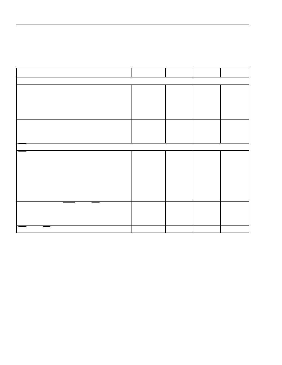
Note: TPO is triggered when VDD reaches between 3.0 V to 4.0 V for the OR3Cxx and between 2.7 V and 3.0 V for the OR3Txxx.
Slave Parallel Mode
Power-on Reset Delay
CCLK Period
Configuration Latency (normal mode):
OR3C/T55
OR3C/T80
OR3T125
TPO
TCCLK
TCL
3.90
40.00
1.94
2.87
4.36
13.10
—
ms
ns
ms
Partial Reconfiguration (explicit mode):
OR3C/T55
OR3C/T80
OR3T125
TPR
1.72
2.04
2.48
—
s/frame
INIT
Timing
INIT
High to CCLK Delay:
Slave Parallel
Slave Serial
Master Serial:
(M3 = 1)
(M3 = 0)
Master Parallel:
(M3 = 1)
(M3 = 0)
TINIT_CCLK
1.00
0.50
4.80
1.00
—
3.40
2.00
16.20
3.60
s
Initialization Latency (PRGM high to INIT high):
OR3C/T55
OR3C/T80
OR3T125
TIL
0.30
0.36
0.45
1.00
1.20
1.50
ms
INIT
High to WR, Asynchronous Peripheral
TINIT_WR
2.00
—
s
Parameter
Symbol
Min
Max
Unit
Timing Characteristics (continued)
Table 59. General Configuration Mode Timing Characteristics (continued)
OR3Cxx Commercial: VDD = 5.0 V ± 5%, 0 °C
< TA < 70 °C; Industrial: VDD = 5.0 V ± 10%, –40 °C < TA < +85 °C.
OR3Txxx Commercial: VDD = 3.0 V to 3.6 V, 0 °C
< TA < 70 °C; Industrial: VDD = 3.0 V to 3.6 V, –40 °C < TA < +85 °C.
相关PDF资料 |
PDF描述 |
|---|---|
| OR3T80-5B432 | FPGA, 484 CLBS, 58000 GATES, PBGA432 |
| OR3T80-5B600 | FPGA, 484 CLBS, 58000 GATES, PBGA600 |
| OR3T80-6B432 | FPGA, 484 CLBS, 58000 GATES, PBGA432 |
| OR3T80-6B600 | FPGA, 484 CLBS, 58000 GATES, PBGA600 |
| OR3T80-4BC432 | FPGA, 484 CLBS, 58000 GATES, 80 MHz, PBGA432 |
相关代理商/技术参数 |
参数描述 |
|---|---|
| OR3T80-4BC432I | 制造商:未知厂家 制造商全称:未知厂家 功能描述:Field Programmable Gate Array (FPGA) |
| OR3T80-4BC600I | 制造商:未知厂家 制造商全称:未知厂家 功能描述:Field Programmable Gate Array (FPGA) |
| OR3T80-4PS208I | 制造商:未知厂家 制造商全称:未知厂家 功能描述:Field Programmable Gate Array (FPGA) |
| OR3T80-4PS240I | 制造商:未知厂家 制造商全称:未知厂家 功能描述:Field Programmable Gate Array (FPGA) |
| OR3T80-5BA352 | 制造商:AGERE 制造商全称:AGERE 功能描述:3C and 3T Field-Programmable Gate Arrays |
发布紧急采购,3分钟左右您将得到回复。