- 您现在的位置:买卖IC网 > PDF目录299577 > OR3T80-4B600 FPGA, 484 CLBS, 58000 GATES, PBGA600 PDF资料下载
参数资料
| 型号: | OR3T80-4B600 |
| 元件分类: | FPGA |
| 英文描述: | FPGA, 484 CLBS, 58000 GATES, PBGA600 |
| 封装: | BGA-600 |
| 文件页数: | 8/210页 |
| 文件大小: | 2138K |
| 代理商: | OR3T80-4B600 |
第1页第2页第3页第4页第5页第6页第7页当前第8页第9页第10页第11页第12页第13页第14页第15页第16页第17页第18页第19页第20页第21页第22页第23页第24页第25页第26页第27页第28页第29页第30页第31页第32页第33页第34页第35页第36页第37页第38页第39页第40页第41页第42页第43页第44页第45页第46页第47页第48页第49页第50页第51页第52页第53页第54页第55页第56页第57页第58页第59页第60页第61页第62页第63页第64页第65页第66页第67页第68页第69页第70页第71页第72页第73页第74页第75页第76页第77页第78页第79页第80页第81页第82页第83页第84页第85页第86页第87页第88页第89页第90页第91页第92页第93页第94页第95页第96页第97页第98页第99页第100页第101页第102页第103页第104页第105页第106页第107页第108页第109页第110页第111页第112页第113页第114页第115页第116页第117页第118页第119页第120页第121页第122页第123页第124页第125页第126页第127页第128页第129页第130页第131页第132页第133页第134页第135页第136页第137页第138页第139页第140页第141页第142页第143页第144页第145页第146页第147页第148页第149页第150页第151页第152页第153页第154页第155页第156页第157页第158页第159页第160页第161页第162页第163页第164页第165页第166页第167页第168页第169页第170页第171页第172页第173页第174页第175页第176页第177页第178页第179页第180页第181页第182页第183页第184页第185页第186页第187页第188页第189页第190页第191页第192页第193页第194页第195页第196页第197页第198页第199页第200页第201页第202页第203页第204页第205页第206页第207页第208页第209页第210页
Preliminary Data Sheet, Rev. 1
September 1998
ORCA Series 3 FPGAs
Lucent Technologies Inc.
105
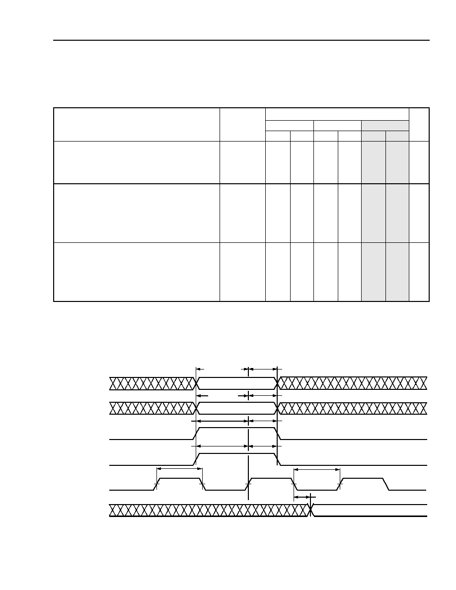
Timing Characteristics (continued)
* The RAM is written on the inactive clock edge following the active edge that latches the address, data, and control signals.
Notes:
Shaded values are advance information and are valid for OR3Txxx devices only.
The table shows worst-case delays. ORCA Foundry reports the delays for individual paths within a group of paths representing the same timing
parameter and may accurately report delays that are less than those listed.
Figure 65. Synchronous Memory Write Characteristics
Table 43. Synchronous Memory Write Characteristics
OR3Cxx Commercial: VDD = 5.0 V ± 5%, 0 °C
< TA < 70 °C; Industrial: VDD = 5.0 V ± 10%, –40 °C < TA < +85 °C.
OR3Txxx Commercial: VDD = 3.0 V to 3.6 V, 0 °C
< TA < 70 °C; Industrial: VDD = 3.0 V to 3.6 V, –40 °C < TA < +85 °C.
Parameter
Symbol
Speed
Unit
-4
-5
-6
Min
Max
Min
Max
Min
Max
Write Operation for RAM Mode:
Maximum Frequency
Clock Low Time
Clock High Time
Clock to Data Valid (CLK to F[6, 4, 2, 0])*
SMCLK_FRQ
SMCLKL_MPW
SMCLKH_MPW
MEM_DEL
151.00
6.77
3.79
—
10.00
197.00
4.97
2.77
—
7.14
266.00
3.49
1.90
—
4.91
MHz
ns
Write Operation Setup Time:
Address to Clock (CIN to CLK)
Address to Clock (DIN[7, 5, 3, 1] to CLK)
Data to Clock (DIN[6, 4, 2, 0] to CLK)
Write Enable (WREN) to Clock (ASWE to CLK)
Write-port Enable 0(WPE0) to Clock (CE to CLK)
Write-port Enable 1(WPE1) to Clock (LSR to CLK)
WA4_SET
WA_SET
WD_SET
WE_SET
WPE0_SET
WPE1_SET
1.25
0.72
0.02
0.18
2.25
2.79
—
0.99
0.52
0.06
0.16
1.69
2.13
—
0.78
0.45
0.12
0.15
1.21
1.58
—
ns
Write Operation Hold Time:
Address from Clock (CIN from CLK)
Address from Clock (DIN[7, 5, 3, 1] from CLK)
Data from Clock (DIN[6, 4, 2, 0] from CLK)
Write Enable (WREN) from Clock (ASWE from CLK)
Write-port Enable 0 (WPE0) from Clock (CE from CLK)
Write-port Enable 1 (WPE1) from Clock (LSR from CLK)
WA4_HLD
WA_HLD
WD_HLD
WE_HLD
WPE0_HLD
WPE1_HLD
0.00
0.59
0.03
0.00
—
0.00
0.42
0.00
—
0.00
0.29
0.00
—
ns
5-4621(F)
CLK
F[6, 4, 2, 0]
CIN, DIN[7, 5, 3, 1]
DIN[6, 4, 2, 0]
MEM_DEL
WA4_SET
ASWE (WREN)
CE (WPE0),
SMCLKH_MPW
WA4_HLD
WD_SET
WD_HLD
WE_SET
WE_HLD
WPE0_SET
WPE0_HLD
WA_SET
WA_HLD
WPE1_SET
WPE1_HLD
LSR (WPE1)
SMCLKH_MPW
相关PDF资料 |
PDF描述 |
|---|---|
| OR3T80-5B432 | FPGA, 484 CLBS, 58000 GATES, PBGA432 |
| OR3T80-5B600 | FPGA, 484 CLBS, 58000 GATES, PBGA600 |
| OR3T80-6B432 | FPGA, 484 CLBS, 58000 GATES, PBGA432 |
| OR3T80-6B600 | FPGA, 484 CLBS, 58000 GATES, PBGA600 |
| OR3T80-4BC432 | FPGA, 484 CLBS, 58000 GATES, 80 MHz, PBGA432 |
相关代理商/技术参数 |
参数描述 |
|---|---|
| OR3T80-4BC432I | 制造商:未知厂家 制造商全称:未知厂家 功能描述:Field Programmable Gate Array (FPGA) |
| OR3T80-4BC600I | 制造商:未知厂家 制造商全称:未知厂家 功能描述:Field Programmable Gate Array (FPGA) |
| OR3T80-4PS208I | 制造商:未知厂家 制造商全称:未知厂家 功能描述:Field Programmable Gate Array (FPGA) |
| OR3T80-4PS240I | 制造商:未知厂家 制造商全称:未知厂家 功能描述:Field Programmable Gate Array (FPGA) |
| OR3T80-5BA352 | 制造商:AGERE 制造商全称:AGERE 功能描述:3C and 3T Field-Programmable Gate Arrays |
发布紧急采购,3分钟左右您将得到回复。