- 您现在的位置:买卖IC网 > PDF目录11732 > ORSO42G5-1BMN484C (Lattice Semiconductor Corporation)IC TRANCEIVERS FPSC 680FPGAM PDF资料下载
参数资料
| 型号: | ORSO42G5-1BMN484C |
| 厂商: | Lattice Semiconductor Corporation |
| 文件页数: | 93/153页 |
| 文件大小: | 0K |
| 描述: | IC TRANCEIVERS FPSC 680FPGAM |
| 产品变化通告: | Product Discontinuation 01/Aug/2011 |
| 标准包装: | 60 |
| 系列: | * |
第1页第2页第3页第4页第5页第6页第7页第8页第9页第10页第11页第12页第13页第14页第15页第16页第17页第18页第19页第20页第21页第22页第23页第24页第25页第26页第27页第28页第29页第30页第31页第32页第33页第34页第35页第36页第37页第38页第39页第40页第41页第42页第43页第44页第45页第46页第47页第48页第49页第50页第51页第52页第53页第54页第55页第56页第57页第58页第59页第60页第61页第62页第63页第64页第65页第66页第67页第68页第69页第70页第71页第72页第73页第74页第75页第76页第77页第78页第79页第80页第81页第82页第83页第84页第85页第86页第87页第88页第89页第90页第91页第92页当前第93页第94页第95页第96页第97页第98页第99页第100页第101页第102页第103页第104页第105页第106页第107页第108页第109页第110页第111页第112页第113页第114页第115页第116页第117页第118页第119页第120页第121页第122页第123页第124页第125页第126页第127页第128页第129页第130页第131页第132页第133页第134页第135页第136页第137页第138页第139页第140页第141页第142页第143页第144页第145页第146页第147页第148页第149页第150页第151页第152页第153页
Lattice Semiconductor
ORCA ORSO42G5 and ORSO82G5 Data Sheet
44
SPE Generator
The SPE generator in the ORSO42G5 and ORSO82G5 is used to indicate the payload and overhead portions of a
SONET frame. It is present in the SONET data path only. The SPE generator generates row, column and STS
counters based on the frame pulse received from the (24 x 33) alignment FIFO or from the descrambler if align-
ment FIFOs are bypassed. It also retimes the 32-bit data in order to align it with the SPE indicator. The SPE gener-
ator will also detect negative or positive pointer justication (if justication is enabled) by looking at the ID bits in the
H1 and H2 bytes and adjust the SPE indicator for the STS-1 frame being justied as follows:
During positive pointer justication, the SPE will be low during H3 byte and the SPE byte following it.
During negative pointer justication, the SPE will be high during H3 byte.
During no justication, the SPE will be low during H3 byte.
This block only detects the incoming pointer bytes for SPE generation. This capability can be enabled by software
control. By default, the SPE generator will ignore any pointer justication. This block has no capability of any
pointer processing, pointer checking or pointer mover operation and ignores “new data” indications from the
SONET specication.
SONET Mode Receive Timing – ORSO42G5
This section contains timing diagrams for major interfaces of this block to the FPGA logic when SONET frames are
to be transferred.
When operating in SONET mode, the entire SONET frame is sent to the FPGA. In multi-channel alignment
mode(s), data from all channels within an alignment group are aligned to the A1A2 framing bytes.
Each SONET frame is 125μs. The frame starts with 36 clock cycles (77.76 MHz) of TOH followed by 1044 clock
cycles of SPE, followed by 36 clock cycles of TOH, 1044 cycles of SPE.
The DOUTxx_SPE signal indicates TOH or SPE in the data (low for TOH, high for SPE)
Twin pairs are AC, AD (group A2) and BC, BD (group B2)
Figure 32 shows the SONET twin alignment mode timing for the ORSO42G5. The frame pulse and SPE indicators
are show for each of the two channels (AC, AD) in twin alignment.
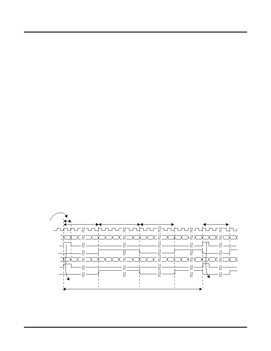
Figure 30. Receive Clocking Diagram for SONET Mode Twin Alignment in Block A – ORSO42G5
RSYSCLKA2
DOUTAC[31:0]
DOUTAC_FP
TT
T
S
SS
T
SSSS
S
...
1 cycle
36 cycles TOH
1
044 cycles SPE
36 cycles TOH
Start of Frame
125 μs
Data
T Represents TOH
S Represents SPE
DOUTxx-SPE is high for SPE, low for TOH
Clocks
RSYSCLKA2 is the read clock used for group A2
RSYSBLKB2 is the read clock used for group B2
36 cycles TOH
TT
T
S
SS
T
SSSS
S
Start of Frame
DOUTAC_SPE
DOUTAD[31:0]
DOUTAD_SPE
DOUTAD_FP
相关PDF资料 |
PDF描述 |
|---|---|
| VE-B03-IX-F1 | CONVERTER MOD DC/DC 24V 75W |
| MS27467T25A61PA | CONN PLUG 61POS STRAIGHT W/PINS |
| MS27467E25A61PA | CONN PLUG 61POS STRAIGHT W/PINS |
| MS27467E25B61PC | CONN PLUG 61POS STRAIGHT W/PINS |
| MM8030-2600RJ3 | CONN MW W/SWITCH 2X2 SMD |
相关代理商/技术参数 |
参数描述 |
|---|---|
| ORSO42G5-1BMN484I | 功能描述:FPGA - 现场可编程门阵列 10368 LUT 204 I/O RoHS:否 制造商:Altera Corporation 系列:Cyclone V E 栅极数量: 逻辑块数量:943 内嵌式块RAM - EBR:1956 kbit 输入/输出端数量:128 最大工作频率:800 MHz 工作电源电压:1.1 V 最大工作温度:+ 70 C 安装风格:SMD/SMT 封装 / 箱体:FBGA-256 |
| ORSO42G5-2BM484C | 功能描述:FPGA - 现场可编程门阵列 10368 LUT 204 I/O RoHS:否 制造商:Altera Corporation 系列:Cyclone V E 栅极数量: 逻辑块数量:943 内嵌式块RAM - EBR:1956 kbit 输入/输出端数量:128 最大工作频率:800 MHz 工作电源电压:1.1 V 最大工作温度:+ 70 C 安装风格:SMD/SMT 封装 / 箱体:FBGA-256 |
| ORSO42G5-2BM484I | 功能描述:FPGA - 现场可编程门阵列 10368 LUT 204 I/O RoHS:否 制造商:Altera Corporation 系列:Cyclone V E 栅极数量: 逻辑块数量:943 内嵌式块RAM - EBR:1956 kbit 输入/输出端数量:128 最大工作频率:800 MHz 工作电源电压:1.1 V 最大工作温度:+ 70 C 安装风格:SMD/SMT 封装 / 箱体:FBGA-256 |
| ORSO42G5-2BMN484C | 功能描述:FPGA - 现场可编程门阵列 10368 LUT 204 I/O RoHS:否 制造商:Altera Corporation 系列:Cyclone V E 栅极数量: 逻辑块数量:943 内嵌式块RAM - EBR:1956 kbit 输入/输出端数量:128 最大工作频率:800 MHz 工作电源电压:1.1 V 最大工作温度:+ 70 C 安装风格:SMD/SMT 封装 / 箱体:FBGA-256 |
| ORSO42G5-2BMN484I | 功能描述:FPGA - 现场可编程门阵列 10368 LUT 204 I/O RoHS:否 制造商:Altera Corporation 系列:Cyclone V E 栅极数量: 逻辑块数量:943 内嵌式块RAM - EBR:1956 kbit 输入/输出端数量:128 最大工作频率:800 MHz 工作电源电压:1.1 V 最大工作温度:+ 70 C 安装风格:SMD/SMT 封装 / 箱体:FBGA-256 |
发布紧急采购,3分钟左右您将得到回复。