- 您现在的位置:买卖IC网 > PDF目录11733 > ORT82G5-2FN680C (Lattice Semiconductor Corporation)IC TRANCEIVERS FPSC 680FPBGA PDF资料下载
参数资料
| 型号: | ORT82G5-2FN680C |
| 厂商: | Lattice Semiconductor Corporation |
| 文件页数: | 62/119页 |
| 文件大小: | 0K |
| 描述: | IC TRANCEIVERS FPSC 680FPBGA |
| 产品变化通告: | Product Discontinuation 01/Aug/2011 |
| 标准包装: | 24 |
| 系列: | * |
第1页第2页第3页第4页第5页第6页第7页第8页第9页第10页第11页第12页第13页第14页第15页第16页第17页第18页第19页第20页第21页第22页第23页第24页第25页第26页第27页第28页第29页第30页第31页第32页第33页第34页第35页第36页第37页第38页第39页第40页第41页第42页第43页第44页第45页第46页第47页第48页第49页第50页第51页第52页第53页第54页第55页第56页第57页第58页第59页第60页第61页当前第62页第63页第64页第65页第66页第67页第68页第69页第70页第71页第72页第73页第74页第75页第76页第77页第78页第79页第80页第81页第82页第83页第84页第85页第86页第87页第88页第89页第90页第91页第92页第93页第94页第95页第96页第97页第98页第99页第100页第101页第102页第103页第104页第105页第106页第107页第108页第109页第110页第111页第112页第113页第114页第115页第116页第117页第118页第119页
Lattice Semiconductor
ORCA ORT42G5 and ORT82G5 Data Sheet
47
The receive channel alignment bypass mode allows mixing of half and full line rates among the channels, as shown
in Figure 28. The gure shows channel pair AA and AB congured in full rate mode at 2.0 Gbps. Channel pair AC
and AD are congured in half-rate mode at 1.0 Gbps.
Figure 28. Receive Clocking for Mixed Line Rates
As noted in the caption of Figure 28, each quad can be congured in any line rate (0.6 to 3.7 Gbps), since each
quad has its own reference clock input pins. The receive alignment FIFO per channel cannot be used in this mode.
Multi-Channel Alignment Clocking Strategies for the ORT82G5
The data on the eight channels (four per SERDES quad) in the ORT82G5 can be independent of each other or can
be synchronized in several ways. For example, two channels within a SERDES can be aligned together; channel A
and B and/or channel C and D. Alternatively, all four channels in a SERDES quad can be aligned together to form a
communication channel with a bandwidth of 10 Gbps. Finally, the alignment can be extended across both SERDES
quads to align all eight channels. Individual channels within an alignment group can be disabled (i.e., powered
down) without disrupting other channels. Clocking strategies for these various modes are described in the following
paragraphs.
For dual alignment both twins within a quad can be sourced by clocks that are different from the other channels,
however each pair of SERDES must have the same clock. The channel pair AA and AB is driven on the low speed
side by RSYS_CLK_A1 and the channel pair AC and AD are driven on the low speed side by RSYS_CLK_A2.
Either RWCKAA or RWCKAB can be connected to RSYS_CLK_A1 and either RWCKAC or RWCKAD can be con-
nected to RSYS_CLK_A2. A clocking example for dual alignment is shown in Figure 29.
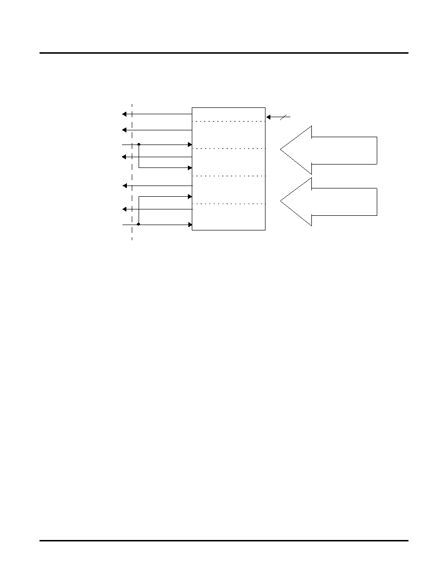
Common Logic, Quad A
Channel AA
Channel AB
Channel AD
Channel AC
REFCLK[P:N]_A
2
100 MHz
RCK78A
RWCKAA
RWCKAC
RSYS_CLK_A1
RSYS_CLK_A2
FPGA
Logic
Two Channels of
2.0 Gbps (Full-Rate)
Incoming Serial Data
25 MHz
RWCKAB
RWCKAD
Recovered
Clocks at
25 MHZ
or 50 MHz
{
Recovered
Clocks at
50 MHZ
{
Two Channels of
1.0 Gbps (Half-Rate)
Incoming Serial Data
相关PDF资料 |
PDF描述 |
|---|---|
| MSP430F4793IPZ | IC MCU 16BIT 60KB FLASH 100LQFP |
| VE-J4B-IW-F3 | CONVERTER MOD DC/DC 95V 100W |
| PIC18F4510-I/ML | IC MCU FLASH 16KX16 44QFN |
| VE-J4B-IW-F2 | CONVERTER MOD DC/DC 95V 100W |
| PIC32MX675F256L-80I/PF | IC MCU 32BIT 256KB FLASH 100TQFP |
相关代理商/技术参数 |
参数描述 |
|---|---|
| ORT82G5-2FN680C1 | 功能描述:FPGA - 现场可编程门阵列 10368 LUT 372 I/O RoHS:否 制造商:Altera Corporation 系列:Cyclone V E 栅极数量: 逻辑块数量:943 内嵌式块RAM - EBR:1956 kbit 输入/输出端数量:128 最大工作频率:800 MHz 工作电源电压:1.1 V 最大工作温度:+ 70 C 安装风格:SMD/SMT 封装 / 箱体:FBGA-256 |
| ORT82G5-2FN680I | 功能描述:FPGA - 现场可编程门阵列 ORCA FPSC 3.7 Gb Bp ln Xcvr 643K Gt I RoHS:否 制造商:Altera Corporation 系列:Cyclone V E 栅极数量: 逻辑块数量:943 内嵌式块RAM - EBR:1956 kbit 输入/输出端数量:128 最大工作频率:800 MHz 工作电源电压:1.1 V 最大工作温度:+ 70 C 安装风格:SMD/SMT 封装 / 箱体:FBGA-256 |
| ORT82G5-2FN680I1 | 功能描述:FPGA - 现场可编程门阵列 10368 LUT 372 I/O RoHS:否 制造商:Altera Corporation 系列:Cyclone V E 栅极数量: 逻辑块数量:943 内嵌式块RAM - EBR:1956 kbit 输入/输出端数量:128 最大工作频率:800 MHz 工作电源电压:1.1 V 最大工作温度:+ 70 C 安装风格:SMD/SMT 封装 / 箱体:FBGA-256 |
| ORT82G5-3BM680C | 功能描述:FPGA - 现场可编程门阵列 10368 LUT 372 I/O RoHS:否 制造商:Altera Corporation 系列:Cyclone V E 栅极数量: 逻辑块数量:943 内嵌式块RAM - EBR:1956 kbit 输入/输出端数量:128 最大工作频率:800 MHz 工作电源电压:1.1 V 最大工作温度:+ 70 C 安装风格:SMD/SMT 封装 / 箱体:FBGA-256 |
| ORT82G5-3BM680C2 | 制造商:LATTICE 制造商全称:Lattice Semiconductor 功能描述:0.6 to 3.7 Gbps XAUI and FC FPSCs |
发布紧急采购,3分钟左右您将得到回复。