- 您现在的位置:买卖IC网 > PDF目录11733 > ORT82G5-2FN680C (Lattice Semiconductor Corporation)IC TRANCEIVERS FPSC 680FPBGA PDF资料下载
参数资料
| 型号: | ORT82G5-2FN680C |
| 厂商: | Lattice Semiconductor Corporation |
| 文件页数: | 75/119页 |
| 文件大小: | 0K |
| 描述: | IC TRANCEIVERS FPSC 680FPBGA |
| 产品变化通告: | Product Discontinuation 01/Aug/2011 |
| 标准包装: | 24 |
| 系列: | * |
第1页第2页第3页第4页第5页第6页第7页第8页第9页第10页第11页第12页第13页第14页第15页第16页第17页第18页第19页第20页第21页第22页第23页第24页第25页第26页第27页第28页第29页第30页第31页第32页第33页第34页第35页第36页第37页第38页第39页第40页第41页第42页第43页第44页第45页第46页第47页第48页第49页第50页第51页第52页第53页第54页第55页第56页第57页第58页第59页第60页第61页第62页第63页第64页第65页第66页第67页第68页第69页第70页第71页第72页第73页第74页当前第75页第76页第77页第78页第79页第80页第81页第82页第83页第84页第85页第86页第87页第88页第89页第90页第91页第92页第93页第94页第95页第96页第97页第98页第99页第100页第101页第102页第103页第104页第105页第106页第107页第108页第109页第110页第111页第112页第113页第114页第115页第116页第117页第118页第119页
Lattice Semiconductor
ORCA ORT42G5 and ORT82G5 Data Sheet
59
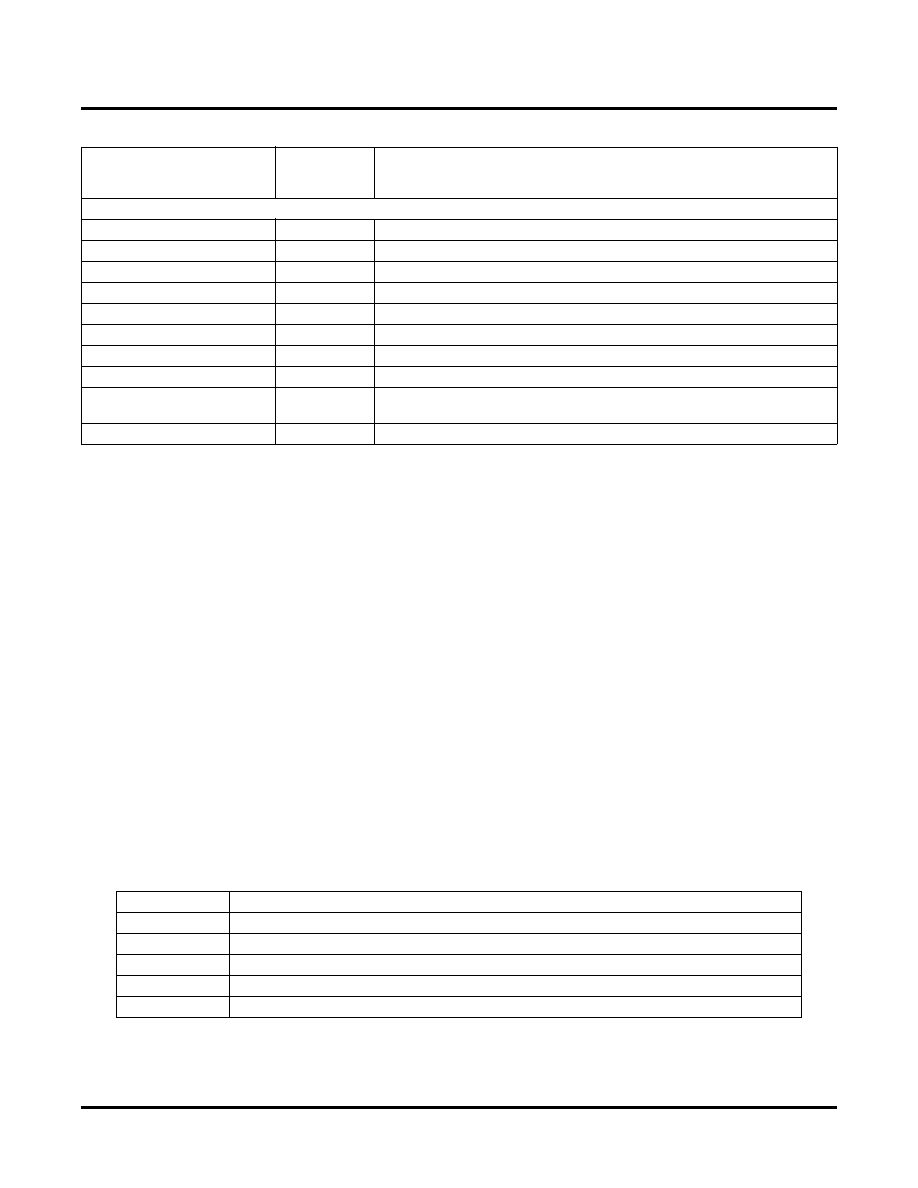
Table 26. Embedded Memory Slice Core/FPGA Interface Signal Description
Memory Maps
Denition of Register Types
The SERDES blocks within the ORT42G5 and ORT82G5 cores have a set of status and control registers for SER-
DES operation. There is also other group of status and control registers which are implemented outside the SER-
DES, which are related to the SERDES and other functional blocks in the FPSC core. (Addresses for the control
and status registers for the FPGA portion of the device are detailed in the ORCA Series 4 FPGAs data sheet,
which also describes the functions of those registers).
ORT42G5 Memory Map
Each ORT42G5 SERDES block has two independent channels. Each channel is identied by both a quad identi-
er, A or B, and a channel identier, C or D. (This naming convention follows that of the ORT82G5.) The registers in
ORT42G5 are 8-bit memory locations, which can be classied into Status Register and Control Register.
Status Register
Read-only register to convey the status information of various operations within the FPSC core. An example is the
state of the XAUI link-state-machine.
Control Register
Read-write register to set up the control inputs that dene the operation of the FPSC core.
Reserved addresses for the FPSC register blocks are shown in Table 29.
Table 27. Structural Register Elements
Table 28 details the memory map for the FPSC portion of the ORT42G5 device. In both Table 29 and Table 28, the
addresses are given as 18-bit hexadecimal (18’h) values. The address may be sourced either through the Micro-
Processor Interface or a User Master Interface. The MicroProcessor Interface (MPI) address bus is a 32-bit bus
FPGA/Embedded Core
Interface Signal Name]
Input (I) to or
Output (O)
from Core
Signal Description
Memory Slice Interface Signals
D_[A:B][35:0]
I
Data in—memory slice [A:B]
CKW_[A:B]
I
Write clock—memory slice [A:B].
CSWA_[A:B]
I
Write chip select for SRAM A—memory slice [A:B].
CSWB_[A:B]
I
Write chip select for SRAM B—memory slice [A:B].
AW_[A:B][10:0]
I
Write address—memory slice [A:B].
BYTEWN_[A:B][3:0]
I
Write control pins for byte-at-a-time write-memory slice [A:B].
Q_[A:B][35:0]
O
Data out—memory slice [A:B].
CKR_[A:B]
I
Read clock—memory slice [A:B].
CSR_[A:B]
I
Read chip select—memory slice [A:B]. CSR_[A:B]= 0 selects SRAM A.
CSR_[A:B]= 1 selects SRAM B.
AR_[A:B][10:0]
I
Read address—memory slice [A:B].
Address (0x)
Description
300xx
SERDES A, internal registers.
301xx
SERDES B, internal registers.
308xx
Channel A [C or D] registers (external to SERDES blocks).
309xx
Channel B [C or D] registers (external to SERDES blocks).
30A0x
Global registers (external to SERDES blocks).
相关PDF资料 |
PDF描述 |
|---|---|
| MSP430F4793IPZ | IC MCU 16BIT 60KB FLASH 100LQFP |
| VE-J4B-IW-F3 | CONVERTER MOD DC/DC 95V 100W |
| PIC18F4510-I/ML | IC MCU FLASH 16KX16 44QFN |
| VE-J4B-IW-F2 | CONVERTER MOD DC/DC 95V 100W |
| PIC32MX675F256L-80I/PF | IC MCU 32BIT 256KB FLASH 100TQFP |
相关代理商/技术参数 |
参数描述 |
|---|---|
| ORT82G5-2FN680C1 | 功能描述:FPGA - 现场可编程门阵列 10368 LUT 372 I/O RoHS:否 制造商:Altera Corporation 系列:Cyclone V E 栅极数量: 逻辑块数量:943 内嵌式块RAM - EBR:1956 kbit 输入/输出端数量:128 最大工作频率:800 MHz 工作电源电压:1.1 V 最大工作温度:+ 70 C 安装风格:SMD/SMT 封装 / 箱体:FBGA-256 |
| ORT82G5-2FN680I | 功能描述:FPGA - 现场可编程门阵列 ORCA FPSC 3.7 Gb Bp ln Xcvr 643K Gt I RoHS:否 制造商:Altera Corporation 系列:Cyclone V E 栅极数量: 逻辑块数量:943 内嵌式块RAM - EBR:1956 kbit 输入/输出端数量:128 最大工作频率:800 MHz 工作电源电压:1.1 V 最大工作温度:+ 70 C 安装风格:SMD/SMT 封装 / 箱体:FBGA-256 |
| ORT82G5-2FN680I1 | 功能描述:FPGA - 现场可编程门阵列 10368 LUT 372 I/O RoHS:否 制造商:Altera Corporation 系列:Cyclone V E 栅极数量: 逻辑块数量:943 内嵌式块RAM - EBR:1956 kbit 输入/输出端数量:128 最大工作频率:800 MHz 工作电源电压:1.1 V 最大工作温度:+ 70 C 安装风格:SMD/SMT 封装 / 箱体:FBGA-256 |
| ORT82G5-3BM680C | 功能描述:FPGA - 现场可编程门阵列 10368 LUT 372 I/O RoHS:否 制造商:Altera Corporation 系列:Cyclone V E 栅极数量: 逻辑块数量:943 内嵌式块RAM - EBR:1956 kbit 输入/输出端数量:128 最大工作频率:800 MHz 工作电源电压:1.1 V 最大工作温度:+ 70 C 安装风格:SMD/SMT 封装 / 箱体:FBGA-256 |
| ORT82G5-3BM680C2 | 制造商:LATTICE 制造商全称:Lattice Semiconductor 功能描述:0.6 to 3.7 Gbps XAUI and FC FPSCs |
发布紧急采购,3分钟左右您将得到回复。