- 您现在的位置:买卖IC网 > PDF目录11733 > ORT82G5-2FN680C (Lattice Semiconductor Corporation)IC TRANCEIVERS FPSC 680FPBGA PDF资料下载
参数资料
| 型号: | ORT82G5-2FN680C |
| 厂商: | Lattice Semiconductor Corporation |
| 文件页数: | 73/119页 |
| 文件大小: | 0K |
| 描述: | IC TRANCEIVERS FPSC 680FPBGA |
| 产品变化通告: | Product Discontinuation 01/Aug/2011 |
| 标准包装: | 24 |
| 系列: | * |
第1页第2页第3页第4页第5页第6页第7页第8页第9页第10页第11页第12页第13页第14页第15页第16页第17页第18页第19页第20页第21页第22页第23页第24页第25页第26页第27页第28页第29页第30页第31页第32页第33页第34页第35页第36页第37页第38页第39页第40页第41页第42页第43页第44页第45页第46页第47页第48页第49页第50页第51页第52页第53页第54页第55页第56页第57页第58页第59页第60页第61页第62页第63页第64页第65页第66页第67页第68页第69页第70页第71页第72页当前第73页第74页第75页第76页第77页第78页第79页第80页第81页第82页第83页第84页第85页第86页第87页第88页第89页第90页第91页第92页第93页第94页第95页第96页第97页第98页第99页第100页第101页第102页第103页第104页第105页第106页第107页第108页第109页第110页第111页第112页第113页第114页第115页第116页第117页第118页第119页
Lattice Semiconductor
ORCA ORT42G5 and ORT82G5 Data Sheet
57
As mentioned earlier, both sections of a slice can be written independently / simultaneously, due to the indepen-
dent CSW per section.
The same signal illustration above applies to slice B by changing _A to _B.
SDRAM A and SDRAM B in Figure 34 refer to the built-in sections A and B of one EAC RAM slice.
These SDRAMS should not be confused with the FPGA SDRAMS, which are generated through Module Generator
in ispLEVER. The EAC SDRAMs are always built-in to the embedded core section of the ORT82G5/42G5 and their
pins are accessed through the EAC interface. In order for these pins to be available at the interface in the gener-
ated HDL models from ispLEVER, the “Use the Extra Memory in FPSC Core” checkbox needs to be checked in the
customization window (after hitting the "customize" button) in Module Generator, while generating the
ORT82G5/42G5 core HDL. These signals will not otherwise show in the interface model.
Figure 35 and Figure 36 show, per slice, timing diagrams for both write and read accesses. These gures do not
include the _x section, which refers to either slice A or B, even though this is implied. Signal names and functions
are summarized in Table 26 and follow the general ORCA Series 4 naming conventions.
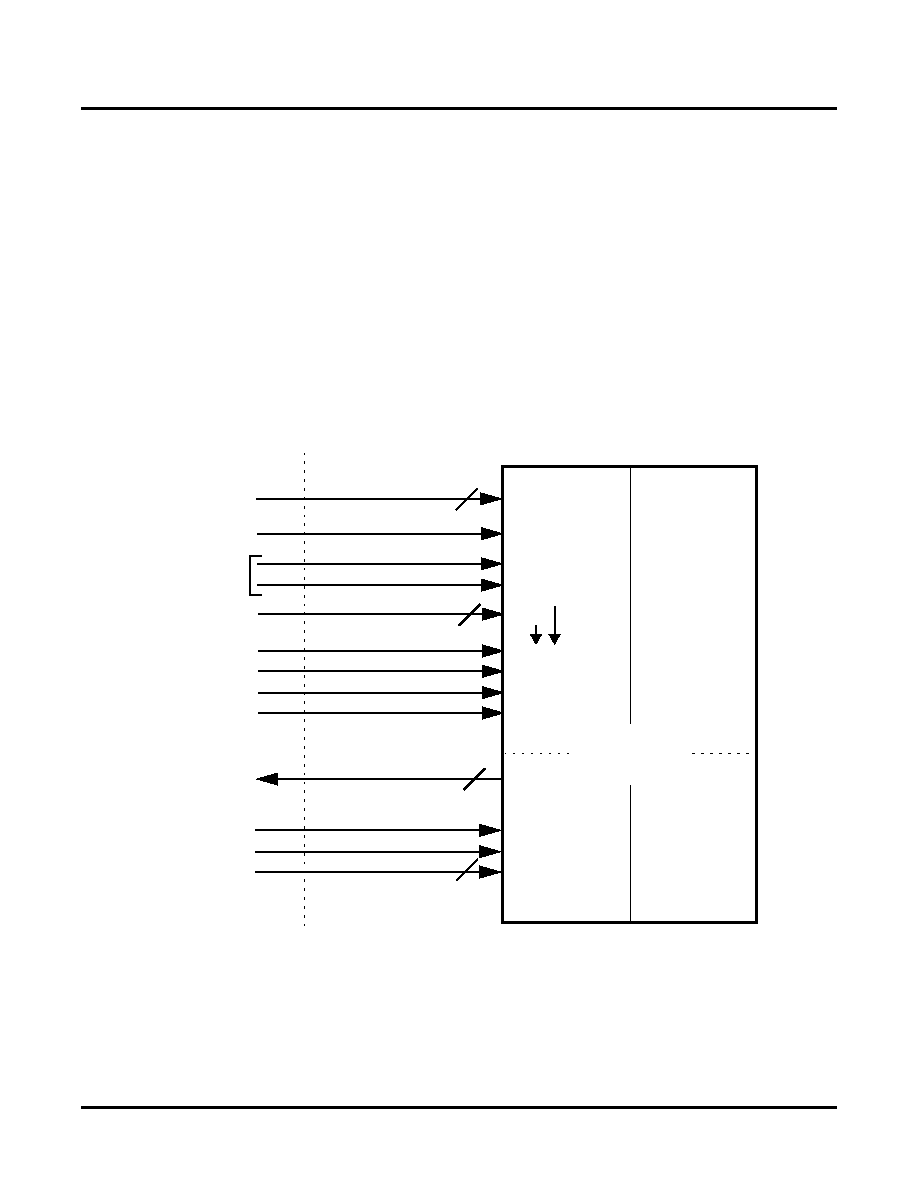
Figure 34. Block Diagram, Embedded Core Memory Slice
4K x 36
D_x[35:0]
Memory Slice
(1 of 2)
2K x 36 Memory
(SRAM A)
(SRAM B)
Write Ports
CKW_x
CSWA_x
CSWB_x
AW_x[10:0]
BYTEWN_x[3]
BW[35,31:24]
BYTEWN_x[2]
BW[34,23:16]
BYTEWN_x[1]
BW[33,15:8]
BYTEWN_x[0]
BW[32,7:0]
Q_x[35:0]
CKR_x
CSR_x
AR_x[10:0]
Read Ports
Side A /
Write Selects
Side B
FPGA
Logic
RAM Block
Read Selects
36
11
36
11
Note: x=[A,B] Slice Identifier
Parity
Data
相关PDF资料 |
PDF描述 |
|---|---|
| MSP430F4793IPZ | IC MCU 16BIT 60KB FLASH 100LQFP |
| VE-J4B-IW-F3 | CONVERTER MOD DC/DC 95V 100W |
| PIC18F4510-I/ML | IC MCU FLASH 16KX16 44QFN |
| VE-J4B-IW-F2 | CONVERTER MOD DC/DC 95V 100W |
| PIC32MX675F256L-80I/PF | IC MCU 32BIT 256KB FLASH 100TQFP |
相关代理商/技术参数 |
参数描述 |
|---|---|
| ORT82G5-2FN680C1 | 功能描述:FPGA - 现场可编程门阵列 10368 LUT 372 I/O RoHS:否 制造商:Altera Corporation 系列:Cyclone V E 栅极数量: 逻辑块数量:943 内嵌式块RAM - EBR:1956 kbit 输入/输出端数量:128 最大工作频率:800 MHz 工作电源电压:1.1 V 最大工作温度:+ 70 C 安装风格:SMD/SMT 封装 / 箱体:FBGA-256 |
| ORT82G5-2FN680I | 功能描述:FPGA - 现场可编程门阵列 ORCA FPSC 3.7 Gb Bp ln Xcvr 643K Gt I RoHS:否 制造商:Altera Corporation 系列:Cyclone V E 栅极数量: 逻辑块数量:943 内嵌式块RAM - EBR:1956 kbit 输入/输出端数量:128 最大工作频率:800 MHz 工作电源电压:1.1 V 最大工作温度:+ 70 C 安装风格:SMD/SMT 封装 / 箱体:FBGA-256 |
| ORT82G5-2FN680I1 | 功能描述:FPGA - 现场可编程门阵列 10368 LUT 372 I/O RoHS:否 制造商:Altera Corporation 系列:Cyclone V E 栅极数量: 逻辑块数量:943 内嵌式块RAM - EBR:1956 kbit 输入/输出端数量:128 最大工作频率:800 MHz 工作电源电压:1.1 V 最大工作温度:+ 70 C 安装风格:SMD/SMT 封装 / 箱体:FBGA-256 |
| ORT82G5-3BM680C | 功能描述:FPGA - 现场可编程门阵列 10368 LUT 372 I/O RoHS:否 制造商:Altera Corporation 系列:Cyclone V E 栅极数量: 逻辑块数量:943 内嵌式块RAM - EBR:1956 kbit 输入/输出端数量:128 最大工作频率:800 MHz 工作电源电压:1.1 V 最大工作温度:+ 70 C 安装风格:SMD/SMT 封装 / 箱体:FBGA-256 |
| ORT82G5-3BM680C2 | 制造商:LATTICE 制造商全称:Lattice Semiconductor 功能描述:0.6 to 3.7 Gbps XAUI and FC FPSCs |
发布紧急采购,3分钟左右您将得到回复。