- 您现在的位置:买卖IC网 > PDF目录367725 > P8xCL580HFT (NXP Semiconductors N.V.) Low voltage 8-bit microcontrollers with UART, I2C-bus and ADC PDF资料下载
参数资料
| 型号: | P8xCL580HFT |
| 厂商: | NXP Semiconductors N.V. |
| 英文描述: | Low voltage 8-bit microcontrollers with UART, I2C-bus and ADC |
| 中文描述: | 低电压8 - UART的,位微控制器的I2C总线和ADC |
| 文件页数: | 8/80页 |
| 文件大小: | 366K |
| 代理商: | P8XCL580HFT |
第1页第2页第3页第4页第5页第6页第7页当前第8页第9页第10页第11页第12页第13页第14页第15页第16页第17页第18页第19页第20页第21页第22页第23页第24页第25页第26页第27页第28页第29页第30页第31页第32页第33页第34页第35页第36页第37页第38页第39页第40页第41页第42页第43页第44页第45页第46页第47页第48页第49页第50页第51页第52页第53页第54页第55页第56页第57页第58页第59页第60页第61页第62页第63页第64页第65页第66页第67页第68页第69页第70页第71页第72页第73页第74页第75页第76页第77页第78页第79页第80页
1997 Mar 14
8
Philips Semiconductors
Product specification
Low voltage 8-bit microcontrollers with
UART, I
2
C-bus and ADC
P80CL580; P83CL580
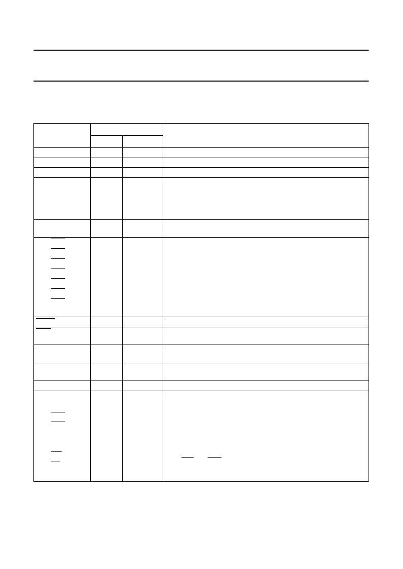
7.2
Pin description
Table 1
For more extensive description of the port pins see Chapter 10 “I/O facilities”.
Pin description for VSO56 (SOT190-1) and QFP64 (SOT319-2)
SYMBOL
PIN
DESCRIPTION
VSO56
QFP64
ADC3 to ADC0
V
ref(p)(A)
V
SSA
P4.0 to P4.7
1 to 4
5
6
7 to 14
59 to 62
63
64
1, 2, 4 to 8,
10
4 input channels to the ADC.
Positive potential of analog-to-digital conversion reference resistor.
Analog part ground.
Port 4
: 8-bit bidirectional I/O port. (P4.0 to P4.7). Port pins that have
logic 1s written to them are pulled HIGH by internal pull-ups, and in this
state can be used as inputs. As inputs, Port 4 pins that are externally
pulled LOW will source current (I
IL
, see Chapter 23) due to the internal
pull-ups. Port 4 output buffers can sink/source 4 LS TTL loads.
Reset
: a HIGH level on this pin for two machine cycles while the
oscillator is running resets the device.
Port 1:
8-bit bidirectional I/O port (P1.0 to P1.7). Same characteristics
as Port 4, but note that P1.6 and P1.7 are open-drain only.
Alternative functions:
– INT2 to INT8 are external interrupt inputs
– STADC is the external trigger of the analog-to-digital converter
– T2 and T2EX are the Timer/event counter 2 inputs
– SCL and SDA are the I
2
C-bus clock and data lines.
RST
15
11
P1.0/INT2/T2
P1.1/INT3/T2EX
P1.2/INT4/STADC
P1.3/INT5
P1.4/INT6
P1.5/INT7
P1.6/INT8/SCL
P1.7/SDA
PWM0
EWN
16
17
18
19
20
21
22
23
24
25
12
13
14
15
16
19
20
21
22
23
Pulse Width Modulation output 0
.
Enable Watchdog Timer
: enable for Watchdog Timer and enable
Power-down mode.
Crystal oscillator output
: output of the inverting amplifier of the
oscillator. Left open when external clock is used.
Crystal oscillator input
: input to the inverting amplifier of the oscillator,
also the input for an externally generated clock source.
Ground: circuit ground potential.
Port 3:
8-bit bidirectional I/O port (P3.0 to P3.7).
Same characteristics as Port 4
Alternative functions:
– RXD is the UART serial data input (asynchronous) or data
input/output (synchronous)
– TXD is the UART serial data output (asynchronous) or clock output
(synchronous)
– INT0 and INT1 are external interrupts 0 and 1
– T0 and T1 are external inputs for timers 0 and 1.
XTAL2
26
24
XTAL1
27
25
V
SS
P3.0/RXD
P3.1/TXD
P3.2/INT0
P3.3/INT1
P3.4/T0
P3.5/T1
P3.6/WR
P3.7/RD
28
29
30
31
32
33
34
35
36
26
27
28
29
30
31
32
33
34
相关PDF资料 |
PDF描述 |
|---|---|
| P8216 | Four-Bit Parallel Bidirectional Bus Driver |
| P8226 | Four-Bit Parallel Bidirectional Bus Driver |
| P82284-6 | CPU System Clock Generator |
| D82284-6 | CPU System Clock Generator |
| D82284-6B | CPU System Clock Generator |
相关代理商/技术参数 |
参数描述 |
|---|---|
| P8Z77 DELUXE | 制造商:Asus 功能描述:P8Z77-V Deluxe ATX Motherboard |
| P8Z77 M PRO | 制造商:Asus 功能描述:P8Z77-M Pro MicroATX Motherboard |
| P8Z77 V | 制造商:Asus 功能描述:P8Z77-V ATX Motherboard |
| P8Z77 V PRO | 制造商:Asus 功能描述:P8Z77-V Pro ATX Motherboard |
| P8Z77-V | 制造商:ASUSTeK Computer Inc 功能描述:P8Z77-V ATX Motherboard |
发布紧急采购,3分钟左右您将得到回复。