- 您现在的位置:买卖IC网 > PDF目录20189 > PCA85132U/2DA/Q1,0 (NXP Semiconductors)IC LCD DRIVER 32 UNCASED PDF资料下载
参数资料
| 型号: | PCA85132U/2DA/Q1,0 |
| 厂商: | NXP Semiconductors |
| 文件页数: | 25/62页 |
| 文件大小: | 0K |
| 描述: | IC LCD DRIVER 32 UNCASED |
| 标准包装: | 600 |
| 显示器类型: | LCD |
| 配置: | 多重 |
| 接口: | I²C |
| 数字或字符: | 任何数字类型 |
| 电流 - 电源: | 60µA |
| 电源电压: | 1.8 V ~ 5.5 V |
| 工作温度: | -40°C ~ 95°C |
| 封装/外壳: | 模具 |
| 供应商设备封装: | 模具 |
| 包装: | 散装 |
第1页第2页第3页第4页第5页第6页第7页第8页第9页第10页第11页第12页第13页第14页第15页第16页第17页第18页第19页第20页第21页第22页第23页第24页当前第25页第26页第27页第28页第29页第30页第31页第32页第33页第34页第35页第36页第37页第38页第39页第40页第41页第42页第43页第44页第45页第46页第47页第48页第49页第50页第51页第52页第53页第54页第55页第56页第57页第58页第59页第60页第61页第62页
�� �
�
�NXP� Semiconductors�
�PCA85132�
�LCD� driver� for� low� multiplex� rates�
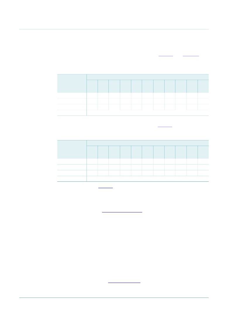
�7.5.3� RAM� writing� in� 1:3� multiplex� drive� mode�
�In� 1:3� multiplex� drive� mode,� the� RAM� is� written� as� shown� in� Table 16� (see� Figure 13� as�
�well).�
�Table� 16.� Standard� RAM� filling� in� 1:3� multiplex� drive� mode�
�Assumption:� BP2/S2,� BP2/S5,� BP2/S8� etc.� are� not� connected� to� any� elements� on� the� display.�
�Display� RAM�
�Display� RAM� addresses� (columns)/segment� outputs� (Sn)�
�bits� (rows)/�
�backplane�
�0�
�1�
�2�
�3�
�4�
�5�
�6�
�7�
�8�
�9�
�:�
�outputs� (BPn)�
�0�
�1�
�2�
�3�
�a7�
�a6�
�a5�
�-�
�a4�
�a3�
�a2�
�-�
�a1�
�a0�
�-�
�-�
�b7�
�b6�
�b5�
�-�
�b4�
�b3�
�b2�
�-�
�b1�
�b0�
�-�
�-�
�c7�
�c6�
�c5�
�-�
�c4�
�c3�
�c2�
�-�
�c1�
�c0�
�-�
�-�
�d7�
�d6�
�d5�
�-�
�:�
�:�
�:�
�:�
�If� the� bit� at� position� BP2/S2� would� be� written� by� a� second� byte� transmitted,� then� the�
��Table� 17.� Entire� RAM� filling� by� rewriting� in� 1:3� multiplex� drive� mode�
�Assumption:� BP2/S2,� BP2/S5,� BP2/S8� etc.� are� connected� to� elements� on� the� display.�
�Display� RAM�
�Display� RAM� addresses� (columns)/segment� outputs� (Sn)�
�bits� (rows)/�
�backplane�
�0�
�1�
�2�
�3�
�4�
�5�
�6�
�7�
�8�
�9�
�:�
�outputs� (BPn)�
�0�
�1�
�a7�
�a6�
�a4�
�a3�
�a1/b7� b4�
�a0/b6� b3�
�b1/c7� c4�
�b0/c6� c3�
�c1/d7� d4�
�c0/d6� d3�
�d1/e7� e4�
�d0/e6� e3�
�:�
�:�
�2�
�3�
�a5�
�-�
�a2�
�-�
�b5�
�-�
�b2�
�-�
�c5�
�-�
�c2�
�-�
�d5�
�-�
�d2�
�-�
�e5�
�-�
�e2�
�-�
�:�
�:�
�In� the� case� described� in� Table 17� the� RAM� has� to� be� written� entirely� and� BP2/S2,� BP2/S5,�
�BP2/S8,� and� so� on,� have� to� be� connected� to� elements� on� the� display.� This� can� be�
�achieved� by� a� combination� of� writing� and� rewriting� the� RAM� like� follows:�
�?� In� the� first� write� to� the� RAM,� bits� a7� to� a0� are� written�
�?� The� data-pointer� (see� Section 7.1.2 on page 7� )� has� to� be� set� to� the� address� of� bit� a1�
�?� In� the� second� write,� bits� b7� to� b0� are� written,� overwriting� bits� a1� and� a0� with� bits� b7�
�and� b6�
�?� The� data-pointer� has� to� be� set� to� the� address� of� bit� b1�
�?� In� the� third� write,� bits� c7� to� c0� are� written,� overwriting� bits� b1� and� b0� with� bits� c7� and�
�c6�
�Depending� on� the� method� of� writing� to� the� RAM� (standard� or� entire� filling� by� rewriting),�
�some� elements� remain� unused� or� can� be� used,� but� it� has� to� be� considered� in� the� module�
�layout� process� as� well� as� in� the� driver� software� design.�
�7.5.4� Bank� selection�
�7.5.4.1�
�Output� bank� selector�
�The� output� bank� selector� (see� Table 10 on page 8� )� selects� one� of� the� four� rows� per� display�
�RAM� address� for� transfer� to� the� display� register.� The� actual� row� selected� depends� on� the�
�particular� LCD� drive� mode� in� operation� and� on� the� instant� in� the� multiplex� sequence.�
�PCA85132�
�Product� data� sheet�
�All� information� provided� in� this� document� is� subject� to� legal� disclaimers.�
�Rev.� 3� —� 11� July� 2013�
�?� NXP� B.V.� 2013.� All� rights� reserved.�
�25� of� 62�
�相关PDF资料 |
PDF描述 |
|---|---|
| EBC19DREH-S13 | CONN EDGECARD 38POS .100 EXTEND |
| RCC12DRYS | CONN EDGECARD 24POS DIP .100 SLD |
| T86C105K050ESAL | CAP TANT 1UF 50V 10% 2312 |
| R2S8-1209 | CONV DC/DC 2W 12VIN 9VOUT SMD |
| IDT71V416L10BEGI8 | IC SRAM 4MBIT 10NS 48FBGA |
相关代理商/技术参数 |
参数描述 |
|---|---|
| PCA85133 | 制造商:PHILIPS 制造商全称:NXP Semiconductors 功能描述:Universal LCD driver for low multiplex rates |
| PCA85133U/2DA/Q1 | 制造商:PHILIPS 制造商全称:NXP Semiconductors 功能描述:Universal LCD driver for low multiplex rates |
| PCA85133U/2DA/Q1,0 | 功能描述:IC LCD DRIVER UNIV UNCASED RoHS:是 类别:未定义的类别 >> 其它 系列:* 标准包装:1 系列:* 其它名称:MS305720A |
| PCA85133U/2DB/Q1 | 制造商:PHILIPS 制造商全称:NXP Semiconductors 功能描述:Universal LCD driver for low multiplex rates |
| PCA85133U/2DB/Q1,0 | 功能描述:IC LCD DRIVER UNIV UNCASED RoHS:是 类别:未定义的类别 >> 其它 系列:* 标准包装:1 系列:* 其它名称:MS305720A |
发布紧急采购,3分钟左右您将得到回复。