- 您现在的位置:买卖IC网 > PDF目录296796 > PCM9211PT (TEXAS INSTRUMENTS INC) DATACOM, TOKEN RING TRANSCEIVER, PQFP48 PDF资料下载
参数资料
| 型号: | PCM9211PT |
| 厂商: | TEXAS INSTRUMENTS INC |
| 元件分类: | 网络接口 |
| 英文描述: | DATACOM, TOKEN RING TRANSCEIVER, PQFP48 |
| 封装: | GREEN, PLASTIC, LQFP-48 |
| 文件页数: | 34/121页 |
| 文件大小: | 1219K |
| 代理商: | PCM9211PT |
第1页第2页第3页第4页第5页第6页第7页第8页第9页第10页第11页第12页第13页第14页第15页第16页第17页第18页第19页第20页第21页第22页第23页第24页第25页第26页第27页第28页第29页第30页第31页第32页第33页当前第34页第35页第36页第37页第38页第39页第40页第41页第42页第43页第44页第45页第46页第47页第48页第49页第50页第51页第52页第53页第54页第55页第56页第57页第58页第59页第60页第61页第62页第63页第64页第65页第66页第67页第68页第69页第70页第71页第72页第73页第74页第75页第76页第77页第78页第79页第80页第81页第82页第83页第84页第85页第86页第87页第88页第89页第90页第91页第92页第93页第94页第95页第96页第97页第98页第99页第100页第101页第102页第103页第104页第105页第106页第107页第108页第109页第110页第111页第112页第113页第114页第115页第116页第117页第118页第119页第120页第121页
SBAS495 – JUNE 2010
www.ti.com
This integrated circuit can be damaged by ESD. Texas Instruments recommends that all integrated circuits be handled with
appropriate precautions. Failure to observe proper handling and installation procedures can cause damage.
ESD damage can range from subtle performance degradation to complete device failure. Precision integrated circuits may be more
susceptible to damage because very small parametric changes could cause the device not to meet its published specifications.
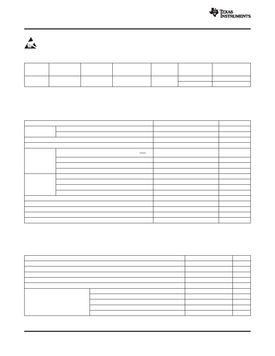
PACKAGE/ORDERING INFORMATION(1)
OPERATING
PACKAGE
TEMPERATURE
PACKAGE
ORDERING
TRANSPORT MEDIA,
PRODUCT
PACKAGE-LEAD
DESIGNATOR
RANGE
MARKING
NUMBER
QUANTITY
PCM9211PT
Tray, 250
PCM9211
LQFP-48
PT
–40°C to +85°C
PCM9211
PCM9211PTR
Tape and Reel, 1000
(1)
For the most current package and ordering information, see the Package Option Addendum at the end of this document, or see the
device product folder on www.ti.com.
ABSOLUTE MAXIMUM RATINGS
(1)
Over operating free-air temperature range (unless otherwise noted).
PCM9211
UNIT
VCC, VDD, VDDRX
–0.3 to +4.0
V
Supply voltage
VCCAD
–0.3 to +6.5
V
Supply voltage differences: VCC, VDD
±0.1
V
Ground voltage differences: AGND, DGND, GNDRX
±0.1
V
RXIN2, RXIN3, RXIN4/ASCKI0, RXIN5/ABCKI0, RXIN6/ALRCKI0,
–0.3 to +6.5
V
RXIN7/ADIN0, MC/SCL, MDI/SDA, MDO/ADR, MS/ADR1, RST
MPIO_A0-A3, MPIO_B0-B3, MPIO_C0-C3
–0.3 to +6.5
V
Digital input voltage
RXIN0, RXIN1 (For S/PDIF TTL / OPTICAL input)
–0.3 to +6.5
V
MODE
–0.3 to +4.0
V
RXIN0, RXIN1 (For S/PDIF Coaxial Input Only)
–0.3 to (VDDRX + 0.3) < +4.0
V
XTI, XTO
–0.3 to (VDD + 0.3) < +4.0
V
Analog input voltage
FILT
–0.3 to (VCC + 0.3) < +4.0
V
VINL, VINR, VCOM
–0.3 to (VCCAD + 0.3) < +6.5
V
Input current (any pins except supplies)
±10
mA
Ambient temperature under bias
–40 to +125
°C
Storage temperature
–55 to +150
°C
Junction temperature
+150
°C
Package temperature (reflow, peak)
+260
°C
(1)
Stresses beyond those listed under Absolute Maximum Ratings may cause permanent damage to the device. These are stress ratings
only and functional operation of the device at these or any other conditions beyond those indicated under Recommended Operating
Conditions is not implied. Exposure to absolute-maximum-rated conditions for extended periods may affect device reliability.
RECOMMENDED OPERATING CONDITIONS
Over operating free-air temperature range (unless otherwise noted).
MIN
NOM
MAX
UNIT
DIR analog supply voltage, VCC
2.9
3.3
3.6
V
ALL digital supply voltage, VDD
2.9
3.3
3.6
V
ADC analog supply voltage, VCCAD
4.5
5.0
5.5
V
Coaxial amplifier supply voltage, VDDRX
2.9
3.3
3.6
V
Digital input interface level
TTL-compatible
DIR, DIT, and Routing sampling frequency
7
216
kHz
DIR, DIT, and Routing system clock frequency
0.896
55.296
MHz
Digital input/output clock frequency
ADC sampling frequency
16
96
kHz
ADC system clock frequency
2.048
24.576
MHz
XTI input clock frequency
24.576
MHz
2
Copyright 2010, Texas Instruments Incorporated
Product Folder Link(s): PCM9211
相关PDF资料 |
PDF描述 |
|---|---|
| PCN11MF | STRIP TERMINAL BLOCK, 1 DECK |
| PCN12E-32S-2.54DSA | 32 CONTACT(S), FEMALE, STRAIGHT TWO PART EURO CONNECTOR, SOLDER, SOCKET |
| PCN12E-44S-2.54DSA | 44 CONTACT(S), FEMALE, STRAIGHT TWO PART EURO CONNECTOR, SOLDER, SOCKET |
| PCN12E-50S-2.54DSA | 50 CONTACT(S), FEMALE, STRAIGHT TWO PART EURO CONNECTOR, SOLDER, SOCKET |
| PCR-E68LMD | 68 CONTACT(S), MALE, RIGHT ANGLE TELECOM AND DATACOM CONNECTOR, SOLDER |
相关代理商/技术参数 |
参数描述 |
|---|---|
| PCM9211PTR | 功能描述:音频发送器、接收器、收发器 216kHz Dig Aud Inter face Transceiver RoHS:否 制造商:Cirrus Logic 工作电源电压:3.3 V, 5 V 电源电流:11.8 mA 通道数量:1 最大工作温度:+ 70 C 接口类型:I2C, SPI 安装风格:SMD/SMT 封装 / 箱体:TSSOP-28 封装: |
| PCM-93 | 功能描述:电线鉴定 Pre-Printed WM Card, Vinyl Cloth, .22" W RoHS:否 制造商:TE Connectivity / Q-Cees 产品:Labels and Signs 类型: 材料:Vinyl 颜色:Blue 宽度:0.625 in 长度:1 in |
| PCM-9342 | 制造商:ADVANTECH 制造商全称:Advantech Co., Ltd. 功能描述:X86 SoC 3.5" SBC with VGA, LCD, LAN, USB, SATA, CF, PC/104 |
| PCM-9342F-64A1E | 制造商:ADVANTECH 制造商全称:Advantech Co., Ltd. 功能描述:X86 SoC 3.5" SBC with VGA, LCD, LAN, USB, SATA, CF, PC/104 |
| PCM-9342FZ2-64A1E | 制造商:ADVANTECH 制造商全称:Advantech Co., Ltd. 功能描述:X86 SoC 3.5" SBC with VGA, LCD, LAN, USB, SATA, CF, PC/104 |
发布紧急采购,3分钟左右您将得到回复。