- 您现在的位置:买卖IC网 > PDF目录98051 > PE33631MLIAA (PEREGRINE SEMICONDUCTOR CORP) PHASE DETECTOR, QCC64 PDF资料下载
参数资料
| 型号: | PE33631MLIAA |
| 厂商: | PEREGRINE SEMICONDUCTOR CORP |
| 元件分类: | PLL合成/DDS/VCOs |
| 英文描述: | PHASE DETECTOR, QCC64 |
| 封装: | 9 X 9 MM, GREEN, QFN-64 |
| 文件页数: | 10/16页 |
| 文件大小: | 295K |
| 代理商: | PE33631MLIAA |
Advance Information
PE33631
Document No. 70-0291-01
│ www.psemi.com
2009 Peregrine Semiconductor Corp. All rights reserved.
Page 3 of 16
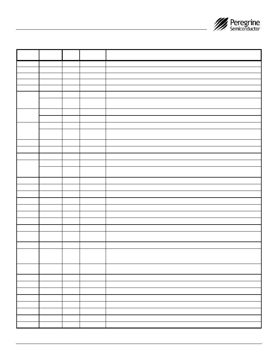
Pin No.
Pin
Name
Valid
Mode
Type
Description
17
VDD
(Note 1)
Digital core VDD.
18
M0
Direct
Input
M Counter bit0 (LSB).
19
M1
Direct
Input
M Counter bit1.
20
M2
Direct
Input
M Counter bit2
21
M3
Direct
Input
M Counter bit3.
22
M4
Direct
Input
M Counter bit4.
S_WR
Serial
Input
Serial load enable input. While S_WR is “low”, Sdata can be serially clocked. Primary register
data are transferred to the secondary register on S_WR rising edge.
23
M5
Direct
Input
M Counter bit5.
SDATA
Serial
Input
Binary serial data input. Input data entered MSB first.
24
M6
Direct
Input
M Counter bit6.
SCLK
Serial
Input
Serial clock input. SDATA is clocked serially into the 21-bit primary register (E_WR “low”) or
the 8-bit enhancement register (E_WR “high”) on the rising edge of Sclk.
25
M7
Direct
Input
M Counter bit7.
26
M8
Direct
Input
M Counter bit8 (MSB).
27
A0
Direct
Input
A Counter bit0 (LSB).
28
A1
Direct
Input
A Counter bit1.
E_WR
Serial
Input
Enhancement register write enable. While E_WR is “high”, Sdata can be serially clocked into
the enhancement register on the rising edge of Sclk.
29
A2
Direct
Input
A Counter bit2.
30
A3
Direct
Input
A Counter bit3 (MSB).
31
DIRECT
Both
Input
Direct mode select. “High” enables direct mode. “Low” enables serial mode.
32
PRE_ENB
Direct
Input
Prescaler enable, active “low”. When “high”, Fin bypasses the prescaler.
33
VDD
(Note 1)
Digital core VDD.
34
GND
Downbond
Ground
35
VDD
(Note 1)
Digital core VDD.
36
Fin
Both
Input
Prescaler input from the VCO. 3.5 GHz max frequency.
37
FinB
Both
Input
Prescaler complementary input. A bypass capacitor should be placed as close as possible to
this pin and be connected in series with a 50
resistor directly to the ground plane.
38
GND
Downbond
Ground
39
CEXT
Both
Output
Logical “NAND” of PD_UB and PD_DB terminated through an on chip, 2 k
series resistor.
Connecting Cext to an external capacitor will low pass filter the input to the inverting amplifier
used for driving LD.
40
LD
Both
Output
Lock detect and open drain logical inversion of CEXT. When the loop is in lock, LD is high
impedance, otherwise LD is a logic low (“0”).
41
DOUT
Both
Output
Data out function, enabled in enhancement mode.
42
VDD
(Note 1)
Output driver/VDD.
43
GND
Downbond
Ground
44
PD_DB
Both
Output
PD_DB pulses down when fp leads fc.
45
GND
Downbond
Ground
46
PD_UB
Both
Output
PD_UB pulses down when fc leads fp.
47
VDD
(Note 1)
Output driver/VDD.
48
VDD
(Note 1)
Phase detector VDD.
Table 1. Pin Descriptions (continued)
相关PDF资料 |
PDF描述 |
|---|---|
| PE33631MLIAA-Z | PHASE DETECTOR, QCC64 |
| PG001M | STEPPER MOTOR CONTROLLER, 0.015 A, PDIP16 |
| PGA308AIDRKR | SPECIALTY ANALOG CIRCUIT, PQCC10 |
| PGA308AIDRKT | SPECIALTY ANALOG CIRCUIT, PQCC10 |
| PGA308AIDGSRG4 | SPECIALTY ANALOG CIRCUIT, PDSO10 |
相关代理商/技术参数 |
参数描述 |
|---|---|
| PE3364 | 制造商:PASTERNACK 制造商全称:Pasternack Enterprises, Inc. 功能描述:CABLE ASSEMBLY RG223/U BNC FEMALE TO BNC FEMALE |
| PE33641 | 制造商:PASTERNACK 制造商全称:Pasternack Enterprises, Inc. 功能描述:CABLE ASSEMBLY RG58C/U SMC PLUG TO SMC PLUG TO SMC PLUG |
| PE33645LF | 制造商:PASTERNACK 制造商全称:Pasternack Enterprises, Inc. 功能描述:CABLE ASSEMBLY RG142B/U SMC PLUG RIGHT ANGLE TO SMC PLUG RIGHT ANGLE(LEAD FREE) |
| PE33646 | 制造商:PASTERNACK 制造商全称:Pasternack Enterprises, Inc. 功能描述:CABLE ASSEMBLY PE-B150 75 OHM SMC PLUG TO 75 OHM BNC MALE |
| PE33646LF | 制造商:PASTERNACK 制造商全称:Pasternack Enterprises, Inc. 功能描述:CABLE ASSEMBLY PE-B150 75 OHM SMC PLUG TO 75 OHM BNC MALE |
发布紧急采购,3分钟左右您将得到回复。