- 您现在的位置:买卖IC网 > PDF目录11641 > PIC10F222-I/OT (Microchip Technology)IC PIC MCU FLASH 512X12 SOT-23-6 PDF资料下载
参数资料
| 型号: | PIC10F222-I/OT |
| 厂商: | Microchip Technology |
| 文件页数: | 16/86页 |
| 文件大小: | 0K |
| 描述: | IC PIC MCU FLASH 512X12 SOT-23-6 |
| 标准包装: | 3,000 |
| 系列: | PIC® 10F |
| 核心处理器: | PIC |
| 芯体尺寸: | 8-位 |
| 速度: | 8MHz |
| 外围设备: | POR,WDT |
| 输入/输出数: | 4 |
| 程序存储器容量: | 768B(512 x 12) |
| 程序存储器类型: | 闪存 |
| RAM 容量: | 23 x 8 |
| 电压 - 电源 (Vcc/Vdd): | 2 V ~ 5.5 V |
| 数据转换器: | A/D 2x8b |
| 振荡器型: | 内部 |
| 工作温度: | -40°C ~ 85°C |
| 封装/外壳: | SOT-23-6 |
| 包装: | 散装 |
第1页第2页第3页第4页第5页第6页第7页第8页第9页第10页第11页第12页第13页第14页第15页当前第16页第17页第18页第19页第20页第21页第22页第23页第24页第25页第26页第27页第28页第29页第30页第31页第32页第33页第34页第35页第36页第37页第38页第39页第40页第41页第42页第43页第44页第45页第46页第47页第48页第49页第50页第51页第52页第53页第54页第55页第56页第57页第58页第59页第60页第61页第62页第63页第64页第65页第66页第67页第68页第69页第70页第71页第72页第73页第74页第75页第76页第77页第78页第79页第80页第81页第82页第83页第84页第85页第86页
2007 Microchip Technology Inc.
DS41270E-page 21
PIC10F220/222
5.0
I/O PORT
As with any other register, the I/O register(s) can be
written and read under program control. However, read
instructions (e.g., MOVF GPIO, W) always read the I/O
pins independent of the pin’s Input/Output modes. On
Reset, all I/O ports are defined as input (inputs are at
high-impedance) since the I/O control registers are all
set.
5.1
GPIO
GPIO is an 8-bit I/O register. Only the low-order 4 bits
are used (GP<3:0>). Bits 7 through 4 are unimple-
mented and read as ‘0’s. Please note that GP3 is an
input only pin. Pins GP0, GP1 and GP3 can be config-
ured with weak pull-ups and also for wake-up on
change. The wake-up on change and weak pull-up
functions are not individually pin selectable. If GP3/
MCLR is configured as MCLR, a weak pull-up can be
enabled via the Configuration Word. Configuring GP3
as MCLR disables the wake-up on change function for
this pin.
5.2
TRIS Registers
The Output Driver Control register is loaded with the
contents of the W register by executing the TRIS f
instruction. A ‘1’ from a TRIS register bit puts the corre-
sponding output driver in a High-Impedance mode. A
‘0’ puts the contents of the output data latch on the
selected pins, enabling the output buffer. The excep-
tions are GP3, which is input only, and the GP2/T0CKI/
FOSC4 pin, which may be controlled by various
registers. See Table 5-1.
The TRIS registers are “write-only” and are set (output
drivers disabled) upon Reset.
5.3
I/O Interfacing
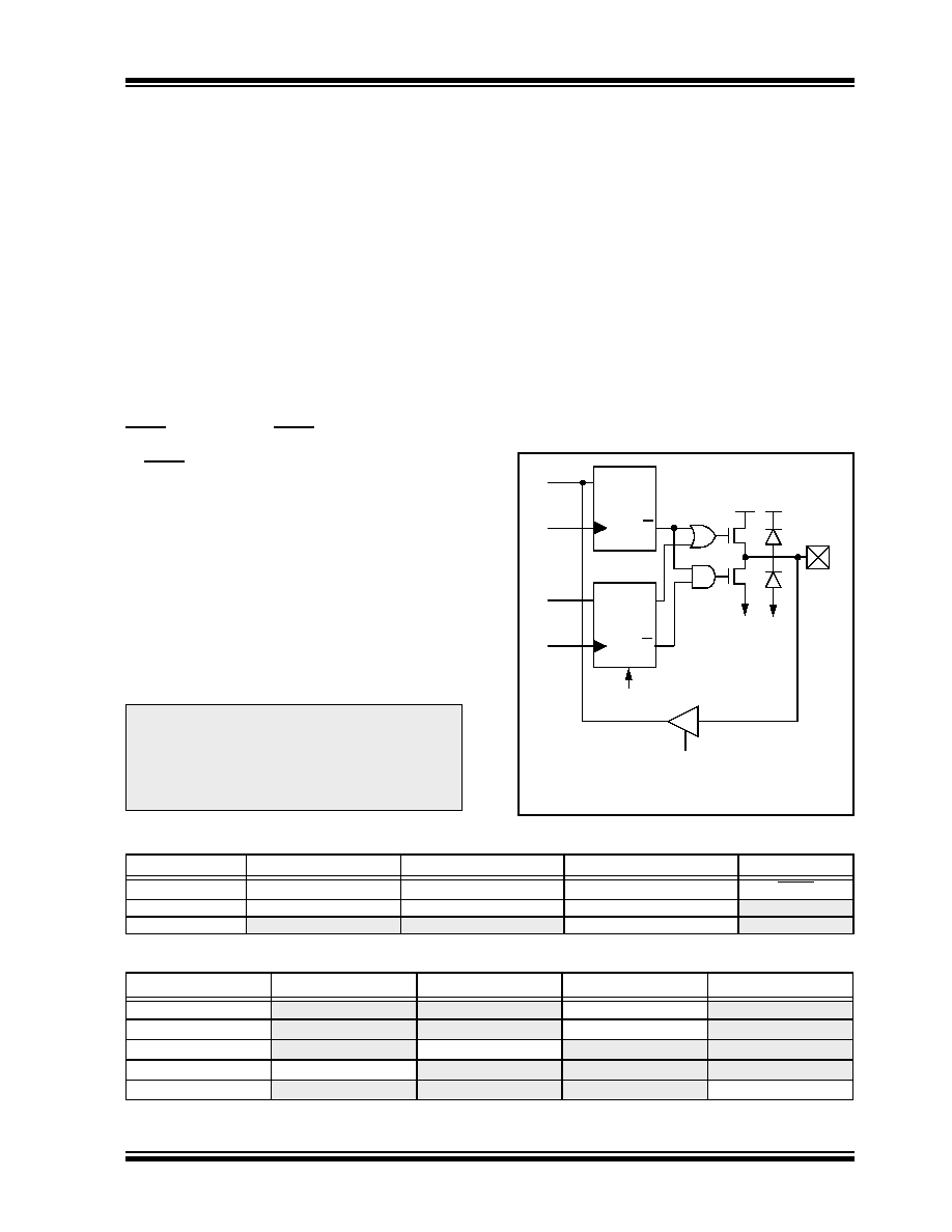
The equivalent circuit for an I/O port pin is shown in
Figure 5-1. All port pins, except GP3, which is input
only, may be used for both input and output operations.
For input operations, these ports are non-latching. Any
input must be present until read by an input instruction
(e.g., MOVF GPIO, W). The outputs are latched and
remain unchanged until the output latch is rewritten. To
use a port pin as output, the corresponding direction
control bit in TRIS must be cleared (= 0). For use as an
input, the corresponding TRIS bit must be set. Any I/O
pin (except GP3) can be programmed individually as
input or output.
FIGURE 5-1:
EQUIVALENT CIRCUIT
FOR A SINGLE I/O PIN
TABLE 5-1:
ORDER OF PRECEDENCE FOR PIN FUNCTIONS
TABLE 5-2:
REQUIREMENTS TO MAKE PINS AVAILABLE IN DIGITAL MODE
Note:
A read of the ports reads the pins, not the
output data latches. That is, if an output
driver on a pin is enabled and driven high,
but the external system is holding it low, a
read of the port will indicate that the pin is
low.
Data
Bus
Q
D
Q
CK
Q
D
Q
CK
P
N
WR
Port
TRIS ‘f’
Data
TRIS
RD Port
VSS
VDD
I/O
pin
W
Reg
Latch
Reset
Note 1:
I/O pins have protection diodes to VDD and
VSS.
2:
See Table 3-1 for buffer type.
VSS
VDD
(2)
(1)
Priority
GP0
GP1
GP2
GP3
1
AN0
AN1
FOSC4
MCLR
2
TRIS GPIO
T0CKI
—
3
—
TRIS GPIO
—
Bit
GP0
GP1
GP2
GP3
FOSC4
—
0
—
T0CS
—
0
—
ANS1
—
0
—
ANS0
0
—
MCLRE
—
0
Legend:
— = Condition of bit will have no effect on the setting of the pin to Digital mode.
相关PDF资料 |
PDF描述 |
|---|---|
| VE-J6P-IY-F4 | CONVERTER MOD DC/DC 13.8V 50W |
| PIC10F220-E/OT | IC PIC MCU FLASH 256X12 SOT-23-6 |
| VE-J6P-IY-F3 | CONVERTER MOD DC/DC 13.8V 50W |
| PIC10F200T-I/MC | IC PIC MCU FLASH 256X12 8DFN |
| VE-J6N-IY-F1 | CONVERTER MOD DC/DC 18.5V 50W |
相关代理商/技术参数 |
参数描述 |
|---|---|
| PIC10F222IP | 制造商:MICROCHIP 制造商全称:Microchip Technology 功能描述:6-Pin, 8-Bit Flash Microcontrollers |
| PIC10F222TE/MC | 制造商:MICROCHIP 制造商全称:Microchip Technology 功能描述:High-Performance Microcontrollers with 8-bit A/D |
| PIC10F222TE/OT | 制造商:MICROCHIP 制造商全称:Microchip Technology 功能描述:High-Performance Microcontrollers with 8-bit A/D |
| PIC10F222T-E/OT | 功能描述:8位微控制器 -MCU 768 B FL 16 RAM RoHS:否 制造商:Silicon Labs 核心:8051 处理器系列:C8051F39x 数据总线宽度:8 bit 最大时钟频率:50 MHz 程序存储器大小:16 KB 数据 RAM 大小:1 KB 片上 ADC:Yes 工作电源电压:1.8 V to 3.6 V 工作温度范围:- 40 C to + 105 C 封装 / 箱体:QFN-20 安装风格:SMD/SMT |
| PIC10F222T-E/OT-CUT TAPE | 制造商:Microchip 功能描述:PIC10 Series 23 B RAM 0.75 KB Flash 8-Bit Flash Microcontroller - SOT-23-6 |
发布紧急采购,3分钟左右您将得到回复。