- 您现在的位置:买卖IC网 > PDF目录11580 > PIC12LF1840-I/MF (Microchip Technology)MCU 7KB FLASH 256B RAM 8-DFN PDF资料下载
参数资料
| 型号: | PIC12LF1840-I/MF |
| 厂商: | Microchip Technology |
| 文件页数: | 15/122页 |
| 文件大小: | 0K |
| 描述: | MCU 7KB FLASH 256B RAM 8-DFN |
| 产品培训模块: | 8-bit PIC® Microcontroller Portfolio |
| 标准包装: | 120 |
| 系列: | PIC® XLP™ 12F |
| 核心处理器: | PIC |
| 芯体尺寸: | 8-位 |
| 速度: | 32MHz |
| 连通性: | I²C,LIN,SPI,UART/USART |
| 外围设备: | 欠压检测/复位,POR,PWM,WDT |
| 输入/输出数: | 5 |
| 程序存储器容量: | 7KB(4K x 14) |
| 程序存储器类型: | 闪存 |
| EEPROM 大小: | 256 x 8 |
| RAM 容量: | 256 x 8 |
| 电压 - 电源 (Vcc/Vdd): | 1.8 V ~ 3.6 V |
| 数据转换器: | A/D 4x10b |
| 振荡器型: | 内部 |
| 工作温度: | -40°C ~ 85°C |
| 封装/外壳: | 8-VDFN 裸露焊盘 |
| 包装: | 管件 |
第1页第2页第3页第4页第5页第6页第7页第8页第9页第10页第11页第12页第13页第14页当前第15页第16页第17页第18页第19页第20页第21页第22页第23页第24页第25页第26页第27页第28页第29页第30页第31页第32页第33页第34页第35页第36页第37页第38页第39页第40页第41页第42页第43页第44页第45页第46页第47页第48页第49页第50页第51页第52页第53页第54页第55页第56页第57页第58页第59页第60页第61页第62页第63页第64页第65页第66页第67页第68页第69页第70页第71页第72页第73页第74页第75页第76页第77页第78页第79页第80页第81页第82页第83页第84页第85页第86页第87页第88页第89页第90页第91页第92页第93页第94页第95页第96页第97页第98页第99页第100页第101页第102页第103页第104页第105页第106页第107页第108页第109页第110页第111页第112页第113页第114页第115页第116页第117页第118页第119页第120页第121页第122页
2011 Microchip Technology Inc.
Preliminary
DS41441B-page 111
PIC12(L)F1840
12.0
I/O PORTS
In general, when a peripheral is enabled, that pin may
not be used as a general purpose I/O pin.
The port has three registers for its operation. These
registers are:
TRISA register (data direction register)
PORTA register (reads the levels on the pins of
the device)
LATA register (output latch)
PORTA has the following additional registers. They
are:
ANSELA (analog select)
WPUA (weak pull-up)
The Data Latch (LATA register) is useful for
read-modify-write operations on the value that the I/O
pins are driving.
A write operation to the LATA register has the same
affect as a write to the corresponding PORTA register.
A read of the LATA register reads of the values held in
the I/O PORT latches, while a read of the PORTA
register reads the actual I/O pin value.
The port has analog functions and has an ANSELA.
register which can disable the digital input and save
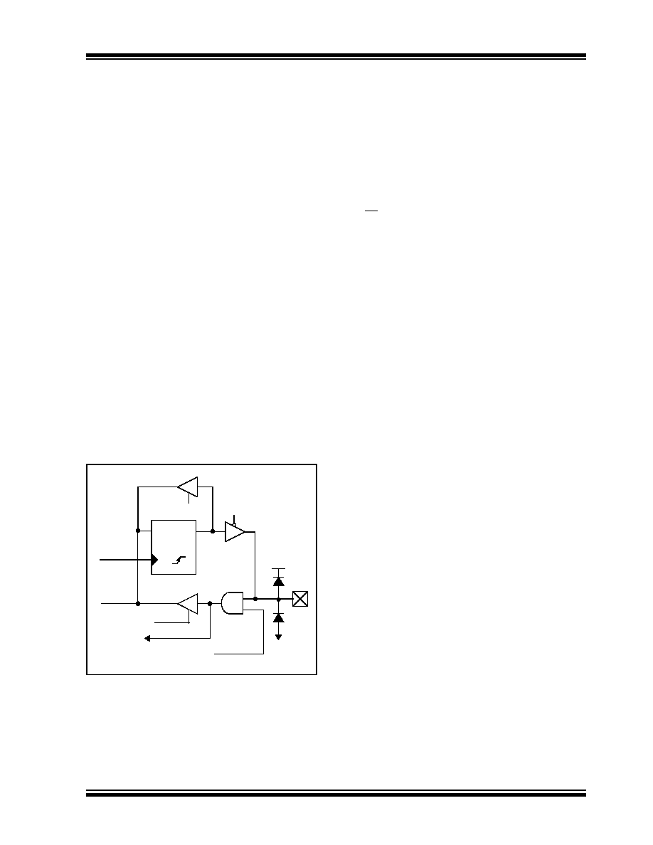
power. A simplified model of a generic I/O port, without
the interfaces to other peripherals, is shown in
FIGURE 12-1:
GENERIC I/O PORT
OPERATION
12.1
Alternate Pin Function
The Alternate Pin Function Control (APFCON) register
is used to steer specific peripheral input and output
functions between different pins. The APFCON register
is shown in Register 12-1. For this device family, the
following functions can be moved between different
pins.
RX/DT
TX/CK
SDO
SS (Slave Select)
T1G
P1B
CCP1/P1A
These bits have no effect on the values of any TRIS
register. PORT and TRIS overrides will be routed to the
correct pin. The unselected pin will be unaffected.
Q
D
CK
Write LATA
Data Register
I/O pin
Read PORTA
Write PORTA
TRISA
Read LATA
Data Bus
To peripherals
ANSELA
VDD
VSS
相关PDF资料 |
PDF描述 |
|---|---|
| V150A36C400BL2 | CONVERTER MOD DC/DC 36V 400W |
| V150A36C400BL | CONVERTER MOD DC/DC 36V 400W |
| V150A36C400B3 | CONVERTER MOD DC/DC 36V 400W |
| V150A36C400B | CONVERTER MOD DC/DC 36V 400W |
| VE-2NN-CV-S | CONVERTER MOD DC/DC 18.5V 150W |
相关代理商/技术参数 |
参数描述 |
|---|---|
| PIC12LF1840T39A-I/ST | 功能描述:8位微控制器 -MCU 7 KB Flash 256 bytes RAM 315-915MHz RoHS:否 制造商:Silicon Labs 核心:8051 处理器系列:C8051F39x 数据总线宽度:8 bit 最大时钟频率:50 MHz 程序存储器大小:16 KB 数据 RAM 大小:1 KB 片上 ADC:Yes 工作电源电压:1.8 V to 3.6 V 工作温度范围:- 40 C to + 105 C 封装 / 箱体:QFN-20 安装风格:SMD/SMT |
| PIC12LF1840T39AT-I/ST | 功能描述:8位微控制器 -MCU 7 KB Flash 256 bytes RAM 315-915MHz RoHS:否 制造商:Silicon Labs 核心:8051 处理器系列:C8051F39x 数据总线宽度:8 bit 最大时钟频率:50 MHz 程序存储器大小:16 KB 数据 RAM 大小:1 KB 片上 ADC:Yes 工作电源电压:1.8 V to 3.6 V 工作温度范围:- 40 C to + 105 C 封装 / 箱体:QFN-20 安装风格:SMD/SMT |
| PIC12LF1840T48A-I/ST | 功能描述:8位微控制器 -MCU 7KB 256bytes RAM 433 -868MHz Tx 6 I/0 Enh RoHS:否 制造商:Silicon Labs 核心:8051 处理器系列:C8051F39x 数据总线宽度:8 bit 最大时钟频率:50 MHz 程序存储器大小:16 KB 数据 RAM 大小:1 KB 片上 ADC:Yes 工作电源电压:1.8 V to 3.6 V 工作温度范围:- 40 C to + 105 C 封装 / 箱体:QFN-20 安装风格:SMD/SMT |
| PIC12LF1840T48AT-I/ST | 功能描述:8位微控制器 -MCU 7KB 256bytes RAM 433 -868MHz Tx 6 I/0 Enh RoHS:否 制造商:Silicon Labs 核心:8051 处理器系列:C8051F39x 数据总线宽度:8 bit 最大时钟频率:50 MHz 程序存储器大小:16 KB 数据 RAM 大小:1 KB 片上 ADC:Yes 工作电源电压:1.8 V to 3.6 V 工作温度范围:- 40 C to + 105 C 封装 / 箱体:QFN-20 安装风格:SMD/SMT |
| PIC12LF1840T-I/MF | 功能描述:8位微控制器 -MCU 7KB Flash EEPROM 256b nanoWatt RoHS:否 制造商:Silicon Labs 核心:8051 处理器系列:C8051F39x 数据总线宽度:8 bit 最大时钟频率:50 MHz 程序存储器大小:16 KB 数据 RAM 大小:1 KB 片上 ADC:Yes 工作电源电压:1.8 V to 3.6 V 工作温度范围:- 40 C to + 105 C 封装 / 箱体:QFN-20 安装风格:SMD/SMT |
发布紧急采购,3分钟左右您将得到回复。