- 您现在的位置:买卖IC网 > PDF目录11580 > PIC12LF1840-I/MF (Microchip Technology)MCU 7KB FLASH 256B RAM 8-DFN PDF资料下载
参数资料
| 型号: | PIC12LF1840-I/MF |
| 厂商: | Microchip Technology |
| 文件页数: | 3/122页 |
| 文件大小: | 0K |
| 描述: | MCU 7KB FLASH 256B RAM 8-DFN |
| 产品培训模块: | 8-bit PIC® Microcontroller Portfolio |
| 标准包装: | 120 |
| 系列: | PIC® XLP™ 12F |
| 核心处理器: | PIC |
| 芯体尺寸: | 8-位 |
| 速度: | 32MHz |
| 连通性: | I²C,LIN,SPI,UART/USART |
| 外围设备: | 欠压检测/复位,POR,PWM,WDT |
| 输入/输出数: | 5 |
| 程序存储器容量: | 7KB(4K x 14) |
| 程序存储器类型: | 闪存 |
| EEPROM 大小: | 256 x 8 |
| RAM 容量: | 256 x 8 |
| 电压 - 电源 (Vcc/Vdd): | 1.8 V ~ 3.6 V |
| 数据转换器: | A/D 4x10b |
| 振荡器型: | 内部 |
| 工作温度: | -40°C ~ 85°C |
| 封装/外壳: | 8-VDFN 裸露焊盘 |
| 包装: | 管件 |
第1页第2页当前第3页第4页第5页第6页第7页第8页第9页第10页第11页第12页第13页第14页第15页第16页第17页第18页第19页第20页第21页第22页第23页第24页第25页第26页第27页第28页第29页第30页第31页第32页第33页第34页第35页第36页第37页第38页第39页第40页第41页第42页第43页第44页第45页第46页第47页第48页第49页第50页第51页第52页第53页第54页第55页第56页第57页第58页第59页第60页第61页第62页第63页第64页第65页第66页第67页第68页第69页第70页第71页第72页第73页第74页第75页第76页第77页第78页第79页第80页第81页第82页第83页第84页第85页第86页第87页第88页第89页第90页第91页第92页第93页第94页第95页第96页第97页第98页第99页第100页第101页第102页第103页第104页第105页第106页第107页第108页第109页第110页第111页第112页第113页第114页第115页第116页第117页第118页第119页第120页第121页第122页
PIC12(L)F1840
DS41441B-page 100
Preliminary
2011 Microchip Technology Inc.
11.3
Flash Program Memory Overview
It is important to understand the Flash program mem-
ory structure for erase and programming operations.
Flash Program memory is arranged in rows. A row con-
sists of a fixed number of 14-bit program memory
words. A row is the minimum block size that can be
erased by user software.
Flash program memory may only be written or erased
if the destination address is in a segment of memory
that is not write-protected, as defined in bits WRT<1:0>
of Configuration Word 2.
After a row has been erased, the user can reprogram
all or a portion of this row. Data to be written into the
program memory row is written to 14-bit wide data write
latches. These write latches are not directly accessible
to the user, but may be loaded via sequential writes to
the EEDATH:EEDATL register pair.
The number of data write latches may not be equivalent
to the number of row locations. During programming,
user software may need to fill the set of write latches
and initiate a programming operation multiple times in
order to fully reprogram an erased row. For example, a
device with a row size of 32 words and eight write
latches will need to load the write latches with data and
initiate a programming operation four times.
The size of a program memory row and the number of
program memory write latches may vary by device.
See Table 11-1 for details.
11.3.1
READING THE FLASH PROGRAM
MEMORY
To read a program memory location, the user must:
1.
Write the Least and Most Significant address
bits to the EEADRH:EEADRL register pair.
2.
Clear the CFGS bit of the EECON1 register.
3.
Set the EEPGD control bit of the EECON1
register.
4.
Then, set control bit RD of the EECON1 register.
Once the read control bit is set, the program memory
Flash controller will use the second instruction cycle to
read the data. This causes the second instruction
immediately following the “BSF EECON1,RD” instruction
to be ignored. The data is available in the very next cycle,
in the EEDATH:EEDATL register pair; therefore, it can
be read as two bytes in the following instructions.
EEDATH:EEDATL register pair will hold this value until
another read or until it is written to by the user.
Note:
If the user wants to modify only a portion
of a previously programmed row, then the
contents of the entire row must be read
and saved in RAM prior to the erase.
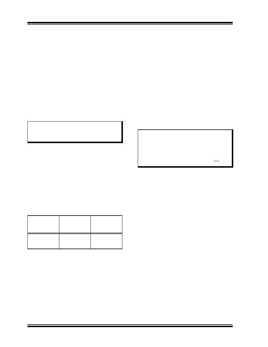
TABLE 11-1:
FLASH MEMORY
ORGANIZATION BY DEVICE
Device
Erase Block
(Row) Size/
Boundary
Number of
Write Latches/
Boundary
PIC12(L)F1840
32 words,
EEADRL<4:0>
= 00000
32 words,
EEADRL<4:0>
= 00000
Note 1:
The two instructions following a program
memory read are required to be NOPs.
This prevents the user from executing a
two-cycle
instruction
on
the
next
instruction after the RD bit is set.
2:
Flash program memory can be read
regardless of the setting of the CP bit.
相关PDF资料 |
PDF描述 |
|---|---|
| V150A36C400BL2 | CONVERTER MOD DC/DC 36V 400W |
| V150A36C400BL | CONVERTER MOD DC/DC 36V 400W |
| V150A36C400B3 | CONVERTER MOD DC/DC 36V 400W |
| V150A36C400B | CONVERTER MOD DC/DC 36V 400W |
| VE-2NN-CV-S | CONVERTER MOD DC/DC 18.5V 150W |
相关代理商/技术参数 |
参数描述 |
|---|---|
| PIC12LF1840T39A-I/ST | 功能描述:8位微控制器 -MCU 7 KB Flash 256 bytes RAM 315-915MHz RoHS:否 制造商:Silicon Labs 核心:8051 处理器系列:C8051F39x 数据总线宽度:8 bit 最大时钟频率:50 MHz 程序存储器大小:16 KB 数据 RAM 大小:1 KB 片上 ADC:Yes 工作电源电压:1.8 V to 3.6 V 工作温度范围:- 40 C to + 105 C 封装 / 箱体:QFN-20 安装风格:SMD/SMT |
| PIC12LF1840T39AT-I/ST | 功能描述:8位微控制器 -MCU 7 KB Flash 256 bytes RAM 315-915MHz RoHS:否 制造商:Silicon Labs 核心:8051 处理器系列:C8051F39x 数据总线宽度:8 bit 最大时钟频率:50 MHz 程序存储器大小:16 KB 数据 RAM 大小:1 KB 片上 ADC:Yes 工作电源电压:1.8 V to 3.6 V 工作温度范围:- 40 C to + 105 C 封装 / 箱体:QFN-20 安装风格:SMD/SMT |
| PIC12LF1840T48A-I/ST | 功能描述:8位微控制器 -MCU 7KB 256bytes RAM 433 -868MHz Tx 6 I/0 Enh RoHS:否 制造商:Silicon Labs 核心:8051 处理器系列:C8051F39x 数据总线宽度:8 bit 最大时钟频率:50 MHz 程序存储器大小:16 KB 数据 RAM 大小:1 KB 片上 ADC:Yes 工作电源电压:1.8 V to 3.6 V 工作温度范围:- 40 C to + 105 C 封装 / 箱体:QFN-20 安装风格:SMD/SMT |
| PIC12LF1840T48AT-I/ST | 功能描述:8位微控制器 -MCU 7KB 256bytes RAM 433 -868MHz Tx 6 I/0 Enh RoHS:否 制造商:Silicon Labs 核心:8051 处理器系列:C8051F39x 数据总线宽度:8 bit 最大时钟频率:50 MHz 程序存储器大小:16 KB 数据 RAM 大小:1 KB 片上 ADC:Yes 工作电源电压:1.8 V to 3.6 V 工作温度范围:- 40 C to + 105 C 封装 / 箱体:QFN-20 安装风格:SMD/SMT |
| PIC12LF1840T-I/MF | 功能描述:8位微控制器 -MCU 7KB Flash EEPROM 256b nanoWatt RoHS:否 制造商:Silicon Labs 核心:8051 处理器系列:C8051F39x 数据总线宽度:8 bit 最大时钟频率:50 MHz 程序存储器大小:16 KB 数据 RAM 大小:1 KB 片上 ADC:Yes 工作电源电压:1.8 V to 3.6 V 工作温度范围:- 40 C to + 105 C 封装 / 箱体:QFN-20 安装风格:SMD/SMT |
发布紧急采购,3分钟左右您将得到回复。