- 您现在的位置:买卖IC网 > PDF目录11239 > PIC16C433/JW (Microchip Technology)IC MCU 2KX14 LIN TXRX 18CDIP PDF资料下载
参数资料
| 型号: | PIC16C433/JW |
| 厂商: | Microchip Technology |
| 文件页数: | 101/126页 |
| 文件大小: | 0K |
| 描述: | IC MCU 2KX14 LIN TXRX 18CDIP |
| 标准包装: | 25 |
| 系列: | PIC® 16C |
| 核心处理器: | PIC |
| 芯体尺寸: | 8-位 |
| 速度: | 10MHz |
| 连通性: | LIN(本地互连网络) |
| 外围设备: | POR,WDT |
| 输入/输出数: | 5 |
| 程序存储器容量: | 3.5KB(2K x 14) |
| 程序存储器类型: | EPROM,UV |
| RAM 容量: | 128 x 8 |
| 电压 - 电源 (Vcc/Vdd): | 4.5 V ~ 5.5 V |
| 数据转换器: | A/D 4x8b |
| 振荡器型: | 内部 |
| 工作温度: | 0°C ~ 70°C |
| 封装/外壳: | 18-CDIP(0.300",7.62mm)窗口 |
| 包装: | 管件 |
| 产品目录页面: | 636 (CN2011-ZH PDF) |
| 配用: | DVA16XP185-ND - ADAPTER DEVICE ICE 18DIP/SOIC |
第1页第2页第3页第4页第5页第6页第7页第8页第9页第10页第11页第12页第13页第14页第15页第16页第17页第18页第19页第20页第21页第22页第23页第24页第25页第26页第27页第28页第29页第30页第31页第32页第33页第34页第35页第36页第37页第38页第39页第40页第41页第42页第43页第44页第45页第46页第47页第48页第49页第50页第51页第52页第53页第54页第55页第56页第57页第58页第59页第60页第61页第62页第63页第64页第65页第66页第67页第68页第69页第70页第71页第72页第73页第74页第75页第76页第77页第78页第79页第80页第81页第82页第83页第84页第85页第86页第87页第88页第89页第90页第91页第92页第93页第94页第95页第96页第97页第98页第99页第100页当前第101页第102页第103页第104页第105页第106页第107页第108页第109页第110页第111页第112页第113页第114页第115页第116页第117页第118页第119页第120页第121页第122页第123页第124页第125页第126页
76
4378C–AVR–09/08
AT90PWM1
13. Timer/Counter0 and Timer/Counter1 Prescalers
Timer/Counter1 and Timer/Counter0 share the same prescaler module, but the Timer/Counters
can have different prescaler settings. The description below applies to both Timer/Counter1 and
Timer/Counter0.
13.0.1
Internal Clock Source
The Timer/Counter can be clocked directly by the system clock (by setting the CSn2:0 = 1). This
provides the fastest operation, with a maximum Timer/Counter clock frequency equal to system
clock frequency (f
CLK_I/O). Alternatively, one of four taps from the prescaler can be used as a
clock source. The prescaled clock has a frequency of either f
CLK_I/O/8, fCLK_I/O/64, fCLK_I/O/256, or
f
CLK_I/O/1024.
13.0.2
Prescaler Reset
The prescaler is free running, i.e., operates independently of the Clock Select logic of the
Timer/Counter, and it is shared by Timer/Counter1 and Timer/Counter0. Since the prescaler is
not affected by the Timer/Counter’s clock select, the state of the prescaler will have implications
for situations where a prescaled clock is used. One example of prescaling artifacts occurs when
the timer is enabled and clocked by the prescaler (6 > CSn2:0 > 1). The number of system clock
cycles from when the timer is enabled to the first count occurs can be from 1 to N+1 system
clock cycles, where N equals the prescaler divisor (8, 64, 256, or 1024).
It is possible to use the prescaler reset for synchronizing the Timer/Counter to program execu-
tion. However, care must be taken if the other Timer/Counter that shares the same prescaler
also uses prescaling. A prescaler reset will affect the prescaler period for all Timer/Counters it is
connected to.
13.0.3
External Clock Source
An external clock source applied to the Tn/T0 pin can be used as Timer/Counter clock
(clk
T1/clkT0). The Tn/T0 pin is sampled once every system clock cycle by the pin synchronization
logic. The synchronized (sampled) signal is then passed through the edge detector. Figure 13-1
shows a functional equivalent block diagram of the Tn/T0 synchronization and edge detector
logic. The registers are clocked at the positive edge of the internal system clock (clk
I/O). The latch
is transparent in the high period of the internal system clock.
The edge detector generates one clk
T1/clkT0 pulse for each positive (CSn2:0 = 7) or negative
(CSn2:0 = 6) edge it detects.
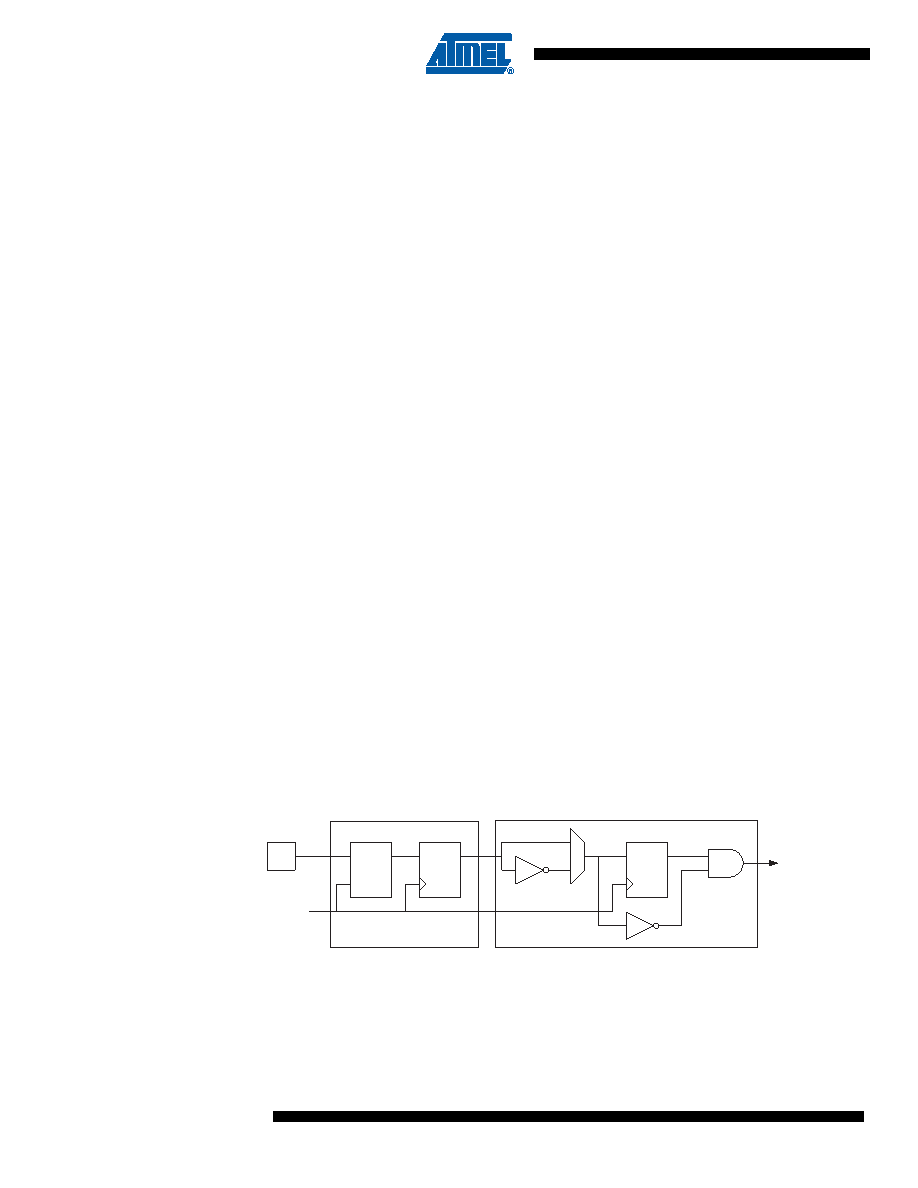
Figure 13-1. Tn/T0 Pin Sampling
The synchronization and edge detector logic introduces a delay of 2.5 to 3.5 system clock cycles
from an edge has been applied to the Tn/T0 pin to the counter is updated.
Enabling and disabling of the clock input must be done when Tn/T0 has been stable for at least
one system clock cycle, otherwise it is a risk that a false Timer/Counter clock pulse is generated.
Tn_sync
(To Clock
Select Logic)
Edge Detector
Synchronization
DQ
LE
DQ
Tn
clk
I/O
相关PDF资料 |
PDF描述 |
|---|---|
| VI-21M-IX-F3 | CONVERTER MOD DC/DC 10V 75W |
| ADG1421BRMZ-REEL7 | IC SW SPST 2.1OHM RON 10MSOP |
| ADG1422BRMZ-REEL7 | IC SW SPST 2.1OHM RON 10MSOP |
| PIC17C44-25I/L | IC MCU OTP 8KX16 PWM 44PLCC |
| CK05BX472K | CAP CER 4700PF 100V 10% RADIAL |
相关代理商/技术参数 |
参数描述 |
|---|---|
| PIC16C433T-E/SO | 功能描述:8位微控制器 -MCU 3.5KB 128 RAM 6 I/O RoHS:否 制造商:Silicon Labs 核心:8051 处理器系列:C8051F39x 数据总线宽度:8 bit 最大时钟频率:50 MHz 程序存储器大小:16 KB 数据 RAM 大小:1 KB 片上 ADC:Yes 工作电源电压:1.8 V to 3.6 V 工作温度范围:- 40 C to + 105 C 封装 / 箱体:QFN-20 安装风格:SMD/SMT |
| PIC16C433T-I/SO | 功能描述:8位微控制器 -MCU 3.5KB 128 RAM 6 I/O RoHS:否 制造商:Silicon Labs 核心:8051 处理器系列:C8051F39x 数据总线宽度:8 bit 最大时钟频率:50 MHz 程序存储器大小:16 KB 数据 RAM 大小:1 KB 片上 ADC:Yes 工作电源电压:1.8 V to 3.6 V 工作温度范围:- 40 C to + 105 C 封装 / 箱体:QFN-20 安装风格:SMD/SMT |
| PIC16C505/JW | 功能描述:8位微控制器 -MCU 1.5KB 72 RAM 12 I/O RoHS:否 制造商:Silicon Labs 核心:8051 处理器系列:C8051F39x 数据总线宽度:8 bit 最大时钟频率:50 MHz 程序存储器大小:16 KB 数据 RAM 大小:1 KB 片上 ADC:Yes 工作电源电压:1.8 V to 3.6 V 工作温度范围:- 40 C to + 105 C 封装 / 箱体:QFN-20 安装风格:SMD/SMT |
| PIC16C505-04/P | 功能描述:8位微控制器 -MCU 1.5KB 72 RAM 12 I/O 4MHz PDIP14 RoHS:否 制造商:Silicon Labs 核心:8051 处理器系列:C8051F39x 数据总线宽度:8 bit 最大时钟频率:50 MHz 程序存储器大小:16 KB 数据 RAM 大小:1 KB 片上 ADC:Yes 工作电源电压:1.8 V to 3.6 V 工作温度范围:- 40 C to + 105 C 封装 / 箱体:QFN-20 安装风格:SMD/SMT |
| PIC16C505-04/P | 制造商:Microchip Technology Inc 功能描述:IC 8BIT CMOS MCU (TUBE 30) 16C505 制造商:Microchip Technology Inc 功能描述:IC 8BIT CMOS MCU 16C505 DIP14 |
发布紧急采购,3分钟左右您将得到回复。