- 您现在的位置:买卖IC网 > PDF目录11239 > PIC16C433/JW (Microchip Technology)IC MCU 2KX14 LIN TXRX 18CDIP PDF资料下载
参数资料
| 型号: | PIC16C433/JW |
| 厂商: | Microchip Technology |
| 文件页数: | 77/126页 |
| 文件大小: | 0K |
| 描述: | IC MCU 2KX14 LIN TXRX 18CDIP |
| 标准包装: | 25 |
| 系列: | PIC® 16C |
| 核心处理器: | PIC |
| 芯体尺寸: | 8-位 |
| 速度: | 10MHz |
| 连通性: | LIN(本地互连网络) |
| 外围设备: | POR,WDT |
| 输入/输出数: | 5 |
| 程序存储器容量: | 3.5KB(2K x 14) |
| 程序存储器类型: | EPROM,UV |
| RAM 容量: | 128 x 8 |
| 电压 - 电源 (Vcc/Vdd): | 4.5 V ~ 5.5 V |
| 数据转换器: | A/D 4x8b |
| 振荡器型: | 内部 |
| 工作温度: | 0°C ~ 70°C |
| 封装/外壳: | 18-CDIP(0.300",7.62mm)窗口 |
| 包装: | 管件 |
| 产品目录页面: | 636 (CN2011-ZH PDF) |
| 配用: | DVA16XP185-ND - ADAPTER DEVICE ICE 18DIP/SOIC |
第1页第2页第3页第4页第5页第6页第7页第8页第9页第10页第11页第12页第13页第14页第15页第16页第17页第18页第19页第20页第21页第22页第23页第24页第25页第26页第27页第28页第29页第30页第31页第32页第33页第34页第35页第36页第37页第38页第39页第40页第41页第42页第43页第44页第45页第46页第47页第48页第49页第50页第51页第52页第53页第54页第55页第56页第57页第58页第59页第60页第61页第62页第63页第64页第65页第66页第67页第68页第69页第70页第71页第72页第73页第74页第75页第76页当前第77页第78页第79页第80页第81页第82页第83页第84页第85页第86页第87页第88页第89页第90页第91页第92页第93页第94页第95页第96页第97页第98页第99页第100页第101页第102页第103页第104页第105页第106页第107页第108页第109页第110页第111页第112页第113页第114页第115页第116页第117页第118页第119页第120页第121页第122页第123页第124页第125页第126页
54
4378C–AVR–09/08
AT90PWM1
Notes:
1. When the BOOTRST Fuse is programmed, the device will jump to the Boot Loader address at
2. When the IVSEL bit in MCUCR is set, Interrupt Vectors will be moved to the start of the Boot
Flash Section. The address of each Interrupt Vector will then be the address in this table
added to the start address of the Boot Flash Section.
Table 6 shows reset and Interrupt Vectors placement for the various combinations of BOOTRST
and IVSEL settings. If the program never enables an interrupt source, the Interrupt Vectors are
not used, and regular program code can be placed at these locations. This is also the case if the
Reset Vector is in the Application section while the Interrupt Vectors are in the Boot section or
vice versa.
Note:
1. The Boot Reset Address is shown in Table 70 on page 218. For the BOOTRST Fuse “1”
means unprogrammed while “0” means programmed.
The most typical and general program setup for the Reset and Interrupt Vector Addresses in
AT90PWM1 is:
Address
Labels Code
Comments
0x000
rjmp
RESET
; Reset Handler
0x001
rjmp
PSC2_CAPT
; PSC2 Capture event Handler
0x002
rjmp
PSC2_EC
; PSC2 End Cycle Handler
0x003
rjmp
PSC1_CAPT
; PSC1 Capture event Handler
0x004
rjmp
PSC1_EC
; PSC1 End Cycle Handler
0x005
rjmp
PSC0_CAPT
; PSC0 Capture event Handler
0x006
rjmp
PSC0_EC
; PSC0 End Cycle Handler
0x007
rjmp
ANA_COMP_0
; Analog Comparator 0 Handler
0x008
rjmp
ANA_COMP_1
; Analog Comparator 1 Handler
0x009
rjmp
ANA_COMP_2
; Analog Comparator 2 Handler
0x00A
rjmp
EXT_INT0
; IRQ0 Handler
0x00B
rjmp
TIM1_CAPT
; Timer1 Capture Handler
0x00C
rjmp
TIM1_COMPA
; Timer1 Compare A Handler
0x00D
rjmp
TIM1_COMPB
; Timer1 Compare B Handler
0x00F
rjmp
TIM1_OVF
; Timer1 Overflow Handler
29
0x001C
INT3
External Interrupt Request 3
30
0x001D
31
0x001E
32
0x001F
SPM READY
Store Program Memory Ready
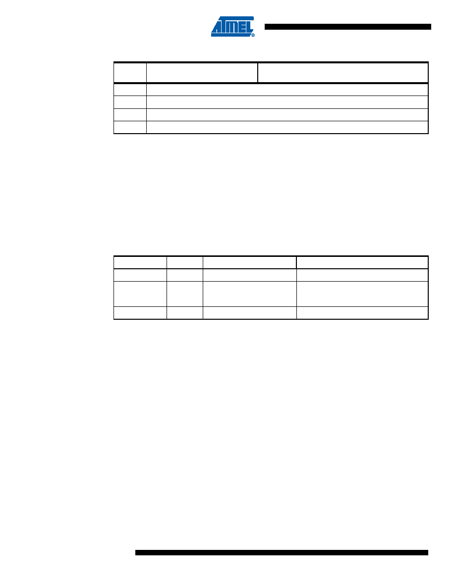
Table 6. Reset and Interrupt Vectors Placement in AT90PWM1
BOOTRST
IVSEL
Reset Address
Interrupt Vectors Start Address
1
0
0x000
0x001
1
0x000
Boot Reset Address + 0x001
0
Boot Reset Address
0x001
0
1
Boot Reset Address
Boot Reset Address + 0x001
Table 5. Reset and Interrupt Vectors
Vector
No.
Program
Address
Source
Interrupt Definition
相关PDF资料 |
PDF描述 |
|---|---|
| VI-21M-IX-F3 | CONVERTER MOD DC/DC 10V 75W |
| ADG1421BRMZ-REEL7 | IC SW SPST 2.1OHM RON 10MSOP |
| ADG1422BRMZ-REEL7 | IC SW SPST 2.1OHM RON 10MSOP |
| PIC17C44-25I/L | IC MCU OTP 8KX16 PWM 44PLCC |
| CK05BX472K | CAP CER 4700PF 100V 10% RADIAL |
相关代理商/技术参数 |
参数描述 |
|---|---|
| PIC16C433T-E/SO | 功能描述:8位微控制器 -MCU 3.5KB 128 RAM 6 I/O RoHS:否 制造商:Silicon Labs 核心:8051 处理器系列:C8051F39x 数据总线宽度:8 bit 最大时钟频率:50 MHz 程序存储器大小:16 KB 数据 RAM 大小:1 KB 片上 ADC:Yes 工作电源电压:1.8 V to 3.6 V 工作温度范围:- 40 C to + 105 C 封装 / 箱体:QFN-20 安装风格:SMD/SMT |
| PIC16C433T-I/SO | 功能描述:8位微控制器 -MCU 3.5KB 128 RAM 6 I/O RoHS:否 制造商:Silicon Labs 核心:8051 处理器系列:C8051F39x 数据总线宽度:8 bit 最大时钟频率:50 MHz 程序存储器大小:16 KB 数据 RAM 大小:1 KB 片上 ADC:Yes 工作电源电压:1.8 V to 3.6 V 工作温度范围:- 40 C to + 105 C 封装 / 箱体:QFN-20 安装风格:SMD/SMT |
| PIC16C505/JW | 功能描述:8位微控制器 -MCU 1.5KB 72 RAM 12 I/O RoHS:否 制造商:Silicon Labs 核心:8051 处理器系列:C8051F39x 数据总线宽度:8 bit 最大时钟频率:50 MHz 程序存储器大小:16 KB 数据 RAM 大小:1 KB 片上 ADC:Yes 工作电源电压:1.8 V to 3.6 V 工作温度范围:- 40 C to + 105 C 封装 / 箱体:QFN-20 安装风格:SMD/SMT |
| PIC16C505-04/P | 功能描述:8位微控制器 -MCU 1.5KB 72 RAM 12 I/O 4MHz PDIP14 RoHS:否 制造商:Silicon Labs 核心:8051 处理器系列:C8051F39x 数据总线宽度:8 bit 最大时钟频率:50 MHz 程序存储器大小:16 KB 数据 RAM 大小:1 KB 片上 ADC:Yes 工作电源电压:1.8 V to 3.6 V 工作温度范围:- 40 C to + 105 C 封装 / 箱体:QFN-20 安装风格:SMD/SMT |
| PIC16C505-04/P | 制造商:Microchip Technology Inc 功能描述:IC 8BIT CMOS MCU (TUBE 30) 16C505 制造商:Microchip Technology Inc 功能描述:IC 8BIT CMOS MCU 16C505 DIP14 |
发布紧急采购,3分钟左右您将得到回复。