- 您现在的位置:买卖IC网 > PDF目录11239 > PIC16C433/JW (Microchip Technology)IC MCU 2KX14 LIN TXRX 18CDIP PDF资料下载
参数资料
| 型号: | PIC16C433/JW |
| 厂商: | Microchip Technology |
| 文件页数: | 108/126页 |
| 文件大小: | 0K |
| 描述: | IC MCU 2KX14 LIN TXRX 18CDIP |
| 标准包装: | 25 |
| 系列: | PIC® 16C |
| 核心处理器: | PIC |
| 芯体尺寸: | 8-位 |
| 速度: | 10MHz |
| 连通性: | LIN(本地互连网络) |
| 外围设备: | POR,WDT |
| 输入/输出数: | 5 |
| 程序存储器容量: | 3.5KB(2K x 14) |
| 程序存储器类型: | EPROM,UV |
| RAM 容量: | 128 x 8 |
| 电压 - 电源 (Vcc/Vdd): | 4.5 V ~ 5.5 V |
| 数据转换器: | A/D 4x8b |
| 振荡器型: | 内部 |
| 工作温度: | 0°C ~ 70°C |
| 封装/外壳: | 18-CDIP(0.300",7.62mm)窗口 |
| 包装: | 管件 |
| 产品目录页面: | 636 (CN2011-ZH PDF) |
| 配用: | DVA16XP185-ND - ADAPTER DEVICE ICE 18DIP/SOIC |
第1页第2页第3页第4页第5页第6页第7页第8页第9页第10页第11页第12页第13页第14页第15页第16页第17页第18页第19页第20页第21页第22页第23页第24页第25页第26页第27页第28页第29页第30页第31页第32页第33页第34页第35页第36页第37页第38页第39页第40页第41页第42页第43页第44页第45页第46页第47页第48页第49页第50页第51页第52页第53页第54页第55页第56页第57页第58页第59页第60页第61页第62页第63页第64页第65页第66页第67页第68页第69页第70页第71页第72页第73页第74页第75页第76页第77页第78页第79页第80页第81页第82页第83页第84页第85页第86页第87页第88页第89页第90页第91页第92页第93页第94页第95页第96页第97页第98页第99页第100页第101页第102页第103页第104页第105页第106页第107页当前第108页第109页第110页第111页第112页第113页第114页第115页第116页第117页第118页第119页第120页第121页第122页第123页第124页第125页第126页
82
4378C–AVR–09/08
AT90PWM1
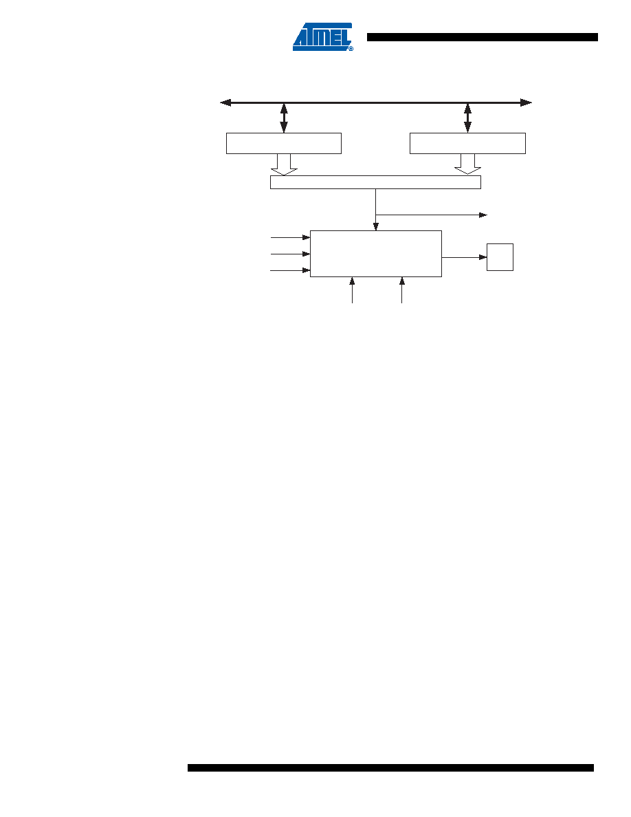
Figure 14-3. Output Compare Unit, Block Diagram
The OCR0x Registers are double buffered when using any of the Pulse Width Modulation
(PWM) modes. For the normal and Clear Timer on Compare (CTC) modes of operation, the dou-
ble buffering is disabled. The double buffering synchronizes the update of the OCR0x Compare
Registers to either top or bottom of the counting sequence. The synchronization prevents the
occurrence of odd-length, non-symmetrical PWM pulses, thereby making the output glitch-free.
The OCR0x Register access may seem complex, but this is not case. When the double buffering
is enabled, the CPU has access to the OCR0x Buffer Register, and if double buffering is dis-
abled the CPU will access the OCR0x directly.
14.4.1
Force Output Compare
In non-PWM waveform generation modes, the match output of the comparator can be forced by
writing a one to the Force Output Compare (FOC0x) bit. Forcing compare match will not set the
OCF0x Flag or reload/clear the timer, but the OC0x pin will be updated as if a real compare
match had occurred (the COM0x1:0 bits settings define whether the OC0x pin is set, cleared or
toggled).
14.4.2
Compare Match Blocking by TCNT0 Write
All CPU write operations to the TCNT0 Register will block any compare match that occur in the
next timer clock cycle, even when the timer is stopped. This feature allows OCR0x to be initial-
ized to the same value as TCNT0 without triggering an interrupt when the Timer/Counter clock is
enabled.
14.4.3
Using the Output Compare Unit
Since writing TCNT0 in any mode of operation will block all compare matches for one timer clock
cycle, there are risks involved when changing TCNT0 when using the Output Compare Unit,
independently of whether the Timer/Counter is running or not. If the value written to TCNT0
equals the OCR0x value, the compare match will be missed, resulting in incorrect waveform
generation. Similarly, do not write the TCNT0 value equal to BOTTOM when the counter is
downcounting.
OCFnx (Int.Req.)
= (8-bit Comparator )
OCRnx
OCnx
DATA BUS
TCNTn
WGMn1:0
Waveform Generator
top
FOCn
COMnx1:0
bottom
相关PDF资料 |
PDF描述 |
|---|---|
| VI-21M-IX-F3 | CONVERTER MOD DC/DC 10V 75W |
| ADG1421BRMZ-REEL7 | IC SW SPST 2.1OHM RON 10MSOP |
| ADG1422BRMZ-REEL7 | IC SW SPST 2.1OHM RON 10MSOP |
| PIC17C44-25I/L | IC MCU OTP 8KX16 PWM 44PLCC |
| CK05BX472K | CAP CER 4700PF 100V 10% RADIAL |
相关代理商/技术参数 |
参数描述 |
|---|---|
| PIC16C433T-E/SO | 功能描述:8位微控制器 -MCU 3.5KB 128 RAM 6 I/O RoHS:否 制造商:Silicon Labs 核心:8051 处理器系列:C8051F39x 数据总线宽度:8 bit 最大时钟频率:50 MHz 程序存储器大小:16 KB 数据 RAM 大小:1 KB 片上 ADC:Yes 工作电源电压:1.8 V to 3.6 V 工作温度范围:- 40 C to + 105 C 封装 / 箱体:QFN-20 安装风格:SMD/SMT |
| PIC16C433T-I/SO | 功能描述:8位微控制器 -MCU 3.5KB 128 RAM 6 I/O RoHS:否 制造商:Silicon Labs 核心:8051 处理器系列:C8051F39x 数据总线宽度:8 bit 最大时钟频率:50 MHz 程序存储器大小:16 KB 数据 RAM 大小:1 KB 片上 ADC:Yes 工作电源电压:1.8 V to 3.6 V 工作温度范围:- 40 C to + 105 C 封装 / 箱体:QFN-20 安装风格:SMD/SMT |
| PIC16C505/JW | 功能描述:8位微控制器 -MCU 1.5KB 72 RAM 12 I/O RoHS:否 制造商:Silicon Labs 核心:8051 处理器系列:C8051F39x 数据总线宽度:8 bit 最大时钟频率:50 MHz 程序存储器大小:16 KB 数据 RAM 大小:1 KB 片上 ADC:Yes 工作电源电压:1.8 V to 3.6 V 工作温度范围:- 40 C to + 105 C 封装 / 箱体:QFN-20 安装风格:SMD/SMT |
| PIC16C505-04/P | 功能描述:8位微控制器 -MCU 1.5KB 72 RAM 12 I/O 4MHz PDIP14 RoHS:否 制造商:Silicon Labs 核心:8051 处理器系列:C8051F39x 数据总线宽度:8 bit 最大时钟频率:50 MHz 程序存储器大小:16 KB 数据 RAM 大小:1 KB 片上 ADC:Yes 工作电源电压:1.8 V to 3.6 V 工作温度范围:- 40 C to + 105 C 封装 / 箱体:QFN-20 安装风格:SMD/SMT |
| PIC16C505-04/P | 制造商:Microchip Technology Inc 功能描述:IC 8BIT CMOS MCU (TUBE 30) 16C505 制造商:Microchip Technology Inc 功能描述:IC 8BIT CMOS MCU 16C505 DIP14 |
发布紧急采购,3分钟左右您将得到回复。