- 您现在的位置:买卖IC网 > PDF目录11239 > PIC16C433/JW (Microchip Technology)IC MCU 2KX14 LIN TXRX 18CDIP PDF资料下载
参数资料
| 型号: | PIC16C433/JW |
| 厂商: | Microchip Technology |
| 文件页数: | 119/126页 |
| 文件大小: | 0K |
| 描述: | IC MCU 2KX14 LIN TXRX 18CDIP |
| 标准包装: | 25 |
| 系列: | PIC® 16C |
| 核心处理器: | PIC |
| 芯体尺寸: | 8-位 |
| 速度: | 10MHz |
| 连通性: | LIN(本地互连网络) |
| 外围设备: | POR,WDT |
| 输入/输出数: | 5 |
| 程序存储器容量: | 3.5KB(2K x 14) |
| 程序存储器类型: | EPROM,UV |
| RAM 容量: | 128 x 8 |
| 电压 - 电源 (Vcc/Vdd): | 4.5 V ~ 5.5 V |
| 数据转换器: | A/D 4x8b |
| 振荡器型: | 内部 |
| 工作温度: | 0°C ~ 70°C |
| 封装/外壳: | 18-CDIP(0.300",7.62mm)窗口 |
| 包装: | 管件 |
| 产品目录页面: | 636 (CN2011-ZH PDF) |
| 配用: | DVA16XP185-ND - ADAPTER DEVICE ICE 18DIP/SOIC |
第1页第2页第3页第4页第5页第6页第7页第8页第9页第10页第11页第12页第13页第14页第15页第16页第17页第18页第19页第20页第21页第22页第23页第24页第25页第26页第27页第28页第29页第30页第31页第32页第33页第34页第35页第36页第37页第38页第39页第40页第41页第42页第43页第44页第45页第46页第47页第48页第49页第50页第51页第52页第53页第54页第55页第56页第57页第58页第59页第60页第61页第62页第63页第64页第65页第66页第67页第68页第69页第70页第71页第72页第73页第74页第75页第76页第77页第78页第79页第80页第81页第82页第83页第84页第85页第86页第87页第88页第89页第90页第91页第92页第93页第94页第95页第96页第97页第98页第99页第100页第101页第102页第103页第104页第105页第106页第107页第108页第109页第110页第111页第112页第113页第114页第115页第116页第117页第118页当前第119页第120页第121页第122页第123页第124页第125页第126页
92
4378C–AVR–09/08
AT90PWM1
Combined with the WGM02 bit found in the TCCR0B Register, these bits control the counting
sequence of the counter, the source for maximum (TOP) counter value, and what type of wave-
form generation to be used, see Table 26. Modes of operation supported by the Timer/Counter
unit are: Normal mode (counter), Clear Timer on Compare Match (CTC) mode, and two types of
Pulse Width Modulation (PWM) modes (see “Modes of Operation” on page 84).
Notes:
1. MAX
= 0xFF
2. BOTTOM = 0x00
14.8.2
Timer/Counter Control Register B – TCCR0B
Bit 7 – FOC0A: Force Output Compare A
The FOC0A bit is only active when the WGM bits specify a non-PWM mode.
However, for ensuring compatibility with future devices, this bit must be set to zero when
TCCR0B is written when operating in PWM mode. When writing a logical one to the FOC0A bit,
an immediate Compare Match is forced on the Waveform Generation unit. The OC0A output is
changed according to its COM0A1:0 bits setting. Note that the FOC0A bit is implemented as a
strobe. Therefore it is the value present in the COM0A1:0 bits that determines the effect of the
forced compare.
A FOC0A strobe will not generate any interrupt, nor will it clear the timer in CTC mode using
OCR0A as TOP.
The FOC0A bit is always read as zero.
Bit 6 – FOC0B: Force Output Compare B
The FOC0B bit is only active when the WGM bits specify a non-PWM mode.
However, for ensuring compatibility with future devices, this bit must be set to zero when
TCCR0B is written when operating in PWM mode. When writing a logical one to the FOC0B bit,
an immediate Compare Match is forced on the Waveform Generation unit. The OC0B output is
changed according to its COM0B1:0 bits setting. Note that the FOC0B bit is implemented as a
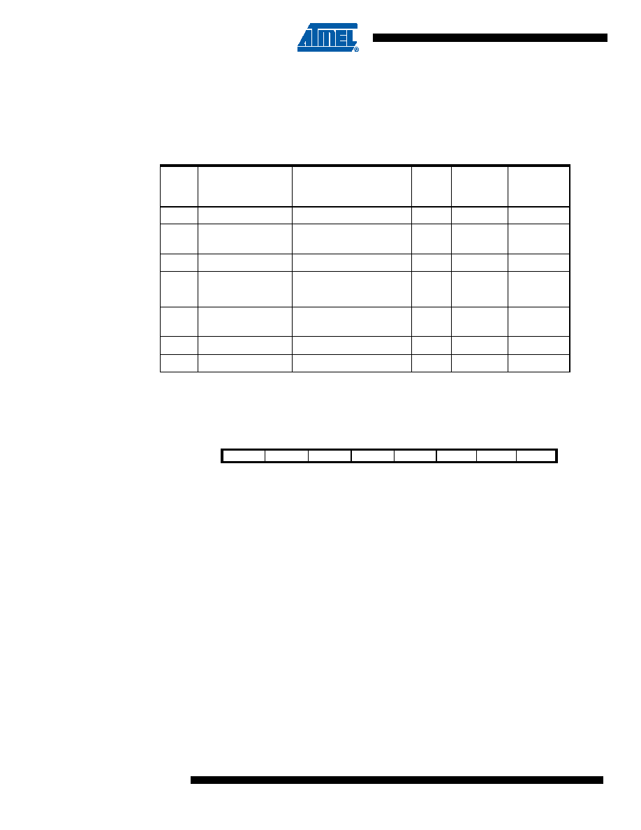
Table 26. Waveform Generation Mode Bit Description
Mode
WGM02
WGM01
WGM00
Timer/Count
er Mode of
Operation
TOP
Update of
OCRx at
TOV Flag
Set on
0
Normal
0xFF
Immediate
MAX
1
001
PWM, Phase
Correct
0xFF
TOP
BOTTOM
2
0
1
0
CTC
OCRA
Immediate
MAX
3
011
Fast PWM
0xFF
TOP
MAX
4
100
Reserved
–
5
101
PWM, Phase
Correct
OCRA
TOP
BOTTOM
6
110
Reserved
–
7
111
Fast PWM
OCRA
TOP
Bit
7
6
5
4
3
2
1
0
FOC0A
FOC0B
–
WGM02
CS02
CS01
CS00
TCCR0B
Read/Write
W
R
R/W
Initial Value
0
相关PDF资料 |
PDF描述 |
|---|---|
| VI-21M-IX-F3 | CONVERTER MOD DC/DC 10V 75W |
| ADG1421BRMZ-REEL7 | IC SW SPST 2.1OHM RON 10MSOP |
| ADG1422BRMZ-REEL7 | IC SW SPST 2.1OHM RON 10MSOP |
| PIC17C44-25I/L | IC MCU OTP 8KX16 PWM 44PLCC |
| CK05BX472K | CAP CER 4700PF 100V 10% RADIAL |
相关代理商/技术参数 |
参数描述 |
|---|---|
| PIC16C433T-E/SO | 功能描述:8位微控制器 -MCU 3.5KB 128 RAM 6 I/O RoHS:否 制造商:Silicon Labs 核心:8051 处理器系列:C8051F39x 数据总线宽度:8 bit 最大时钟频率:50 MHz 程序存储器大小:16 KB 数据 RAM 大小:1 KB 片上 ADC:Yes 工作电源电压:1.8 V to 3.6 V 工作温度范围:- 40 C to + 105 C 封装 / 箱体:QFN-20 安装风格:SMD/SMT |
| PIC16C433T-I/SO | 功能描述:8位微控制器 -MCU 3.5KB 128 RAM 6 I/O RoHS:否 制造商:Silicon Labs 核心:8051 处理器系列:C8051F39x 数据总线宽度:8 bit 最大时钟频率:50 MHz 程序存储器大小:16 KB 数据 RAM 大小:1 KB 片上 ADC:Yes 工作电源电压:1.8 V to 3.6 V 工作温度范围:- 40 C to + 105 C 封装 / 箱体:QFN-20 安装风格:SMD/SMT |
| PIC16C505/JW | 功能描述:8位微控制器 -MCU 1.5KB 72 RAM 12 I/O RoHS:否 制造商:Silicon Labs 核心:8051 处理器系列:C8051F39x 数据总线宽度:8 bit 最大时钟频率:50 MHz 程序存储器大小:16 KB 数据 RAM 大小:1 KB 片上 ADC:Yes 工作电源电压:1.8 V to 3.6 V 工作温度范围:- 40 C to + 105 C 封装 / 箱体:QFN-20 安装风格:SMD/SMT |
| PIC16C505-04/P | 功能描述:8位微控制器 -MCU 1.5KB 72 RAM 12 I/O 4MHz PDIP14 RoHS:否 制造商:Silicon Labs 核心:8051 处理器系列:C8051F39x 数据总线宽度:8 bit 最大时钟频率:50 MHz 程序存储器大小:16 KB 数据 RAM 大小:1 KB 片上 ADC:Yes 工作电源电压:1.8 V to 3.6 V 工作温度范围:- 40 C to + 105 C 封装 / 箱体:QFN-20 安装风格:SMD/SMT |
| PIC16C505-04/P | 制造商:Microchip Technology Inc 功能描述:IC 8BIT CMOS MCU (TUBE 30) 16C505 制造商:Microchip Technology Inc 功能描述:IC 8BIT CMOS MCU 16C505 DIP14 |
发布紧急采购,3分钟左右您将得到回复。