- 您现在的位置:买卖IC网 > PDF目录11590 > PIC16F676-E/P (Microchip Technology)IC MCU FLASH 1KX14 W/AD 14DIP PDF资料下载
参数资料
| 型号: | PIC16F676-E/P |
| 厂商: | Microchip Technology |
| 文件页数: | 58/132页 |
| 文件大小: | 0K |
| 描述: | IC MCU FLASH 1KX14 W/AD 14DIP |
| 产品培训模块: | Asynchronous Stimulus |
| 标准包装: | 30 |
| 系列: | PIC® 16F |
| 核心处理器: | PIC |
| 芯体尺寸: | 8-位 |
| 速度: | 20MHz |
| 外围设备: | 欠压检测/复位,POR,WDT |
| 输入/输出数: | 12 |
| 程序存储器容量: | 1.75KB(1K x 14) |
| 程序存储器类型: | 闪存 |
| EEPROM 大小: | 128 x 8 |
| RAM 容量: | 64 x 8 |
| 电压 - 电源 (Vcc/Vdd): | 2 V ~ 5.5 V |
| 数据转换器: | A/D 8x10b |
| 振荡器型: | 内部 |
| 工作温度: | -40°C ~ 125°C |
| 封装/外壳: | 14-DIP(0.300",7.62mm) |
| 包装: | 管件 |
| 配用: | DM163029-ND - BOARD PICDEM FOR MECHATRONICS |
第1页第2页第3页第4页第5页第6页第7页第8页第9页第10页第11页第12页第13页第14页第15页第16页第17页第18页第19页第20页第21页第22页第23页第24页第25页第26页第27页第28页第29页第30页第31页第32页第33页第34页第35页第36页第37页第38页第39页第40页第41页第42页第43页第44页第45页第46页第47页第48页第49页第50页第51页第52页第53页第54页第55页第56页第57页当前第58页第59页第60页第61页第62页第63页第64页第65页第66页第67页第68页第69页第70页第71页第72页第73页第74页第75页第76页第77页第78页第79页第80页第81页第82页第83页第84页第85页第86页第87页第88页第89页第90页第91页第92页第93页第94页第95页第96页第97页第98页第99页第100页第101页第102页第103页第104页第105页第106页第107页第108页第109页第110页第111页第112页第113页第114页第115页第116页第117页第118页第119页第120页第121页第122页第123页第124页第125页第126页第127页第128页第129页第130页第131页第132页
2010 Microchip Technology Inc.
DS40039F-page 31
PIC16F630/676
4.0
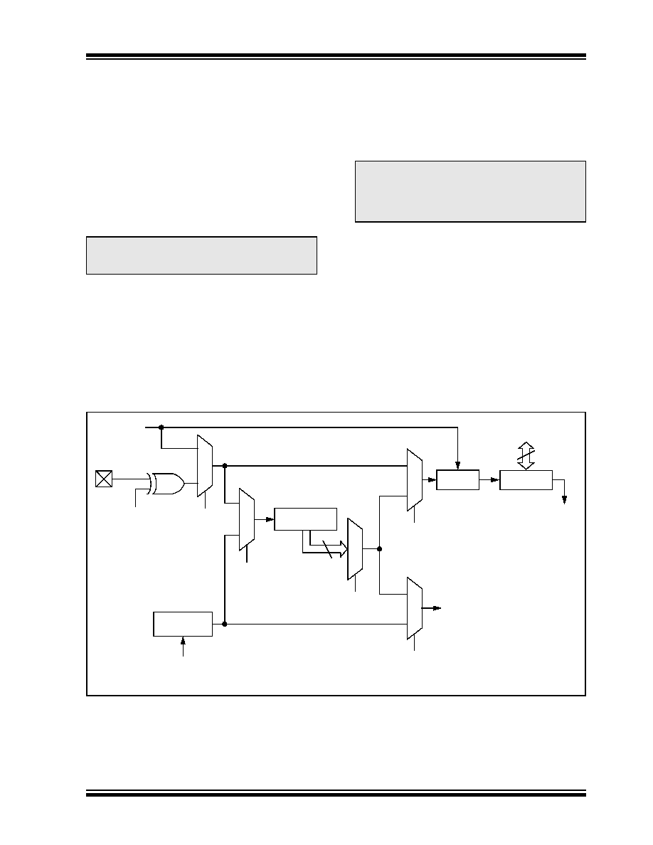
TIMER0 MODULE
The Timer0 module timer/counter has the following
features:
8-bit timer/counter
Readable and writable
8-bit software programmable prescaler
Internal or external clock select
Interrupt on overflow from FFh to 00h
Edge select for external clock
Figure 4-1 is a block diagram of the Timer0 module and
the prescaler shared with the WDT.
4.1
Timer0 Operation
Timer mode is selected by clearing the T0CS bit
(OPTION_REG<5>). In Timer mode, the Timer0
module will increment every instruction cycle (without
prescaler). If TMR0 is written, the increment is inhibited
for the following two instruction cycles. The user can
work around this by writing an adjusted value to the
TMR0 register.
Counter mode is selected by setting the T0CS bit
(OPTION_REG<5>). In this mode, the Timer0 module
will increment either on every rising or falling edge of
pin RA2/T0CKI. The incrementing edge is determined
by
the
source
edge
(T0SE)
control
bit
(OPTION_REG<4>). Clearing the T0SE bit selects the
rising edge.
4.2
Timer0 Interrupt
A Timer0 interrupt is generated when the TMR0
register timer/counter overflows from FFh to 00h. This
overflow sets the T0IF bit. The interrupt can be masked
by clearing the T0IE bit (INTCON<5>). The T0IF bit
(INTCON<2>) must be cleared in software by the
Timer0 module Interrupt Service Routine before re-
enabling this interrupt. The Timer0 interrupt cannot
wake the processor from Sleep since the timer is shut-
off during Sleep.
FIGURE 4-1:
BLOCK DIAGRAM OF THE TIMER0/WDT PRESCALER
Note:
Additional information on the Timer0
module is available in the PIC Mid-Range
Reference Manual, (DS33023).
Note:
Counter mode has specific external clock
requirements. Additional information on
these requirements is available in the PIC
Mid-Range
Reference
Manual,
(DS33023).
T0CKI
T0SE
pin
CLKOUT
TMR0
Watchdog
Timer
WDT
Time-out
PS0 - PS2
WDTE
Data Bus
Set Flag bit T0IF
on Overflow
T0CS
Note 1: T0SE, T0CS, PSA, PS0-PS2 are bits in the OPTION register.
0
1
0
1
0
1
SYNC 2
Cycles
8
8-bit
Prescaler
0
1
(= FOSC/4)
PSA
相关PDF资料 |
PDF描述 |
|---|---|
| PIC12LCE518-04/SN | IC MCU OTP 512X12 LV W/EE 8SOIC |
| PIC12CE518-04I/SM | IC MCU OTP 512X12 W/EE 8-SOIC |
| PIC16LF1829T-I/ML | MCU PIC 14KB FLASH 20-QFN |
| PIC16F1829T-I/ML | MCU PIC 14K FLASH 1K RAM 20QFN |
| PIC16F716-E/ML | IC PIC MCU FLASH 2KX14 28QFN |
相关代理商/技术参数 |
参数描述 |
|---|---|
| PIC16F676-I/ML | 功能描述:8位微控制器 -MCU 1.75 KB 64 RAM 12I/O RoHS:否 制造商:Silicon Labs 核心:8051 处理器系列:C8051F39x 数据总线宽度:8 bit 最大时钟频率:50 MHz 程序存储器大小:16 KB 数据 RAM 大小:1 KB 片上 ADC:Yes 工作电源电压:1.8 V to 3.6 V 工作温度范围:- 40 C to + 105 C 封装 / 箱体:QFN-20 安装风格:SMD/SMT |
| PIC16F676-I/P | 功能描述:8位微控制器 -MCU 1.75KB 64 RAM 12 I/O Ind Temp PDIP14 RoHS:否 制造商:Silicon Labs 核心:8051 处理器系列:C8051F39x 数据总线宽度:8 bit 最大时钟频率:50 MHz 程序存储器大小:16 KB 数据 RAM 大小:1 KB 片上 ADC:Yes 工作电源电压:1.8 V to 3.6 V 工作温度范围:- 40 C to + 105 C 封装 / 箱体:QFN-20 安装风格:SMD/SMT |
| PIC16F676-I/P | 制造商:Microchip Technology Inc 功能描述:IC 8BIT FLASH MCU 16F676 DIP14 |
| PIC16F676-I/SL | 功能描述:8位微控制器 -MCU 1.75KB 64 RAM 12 I/O Ind Temp SOIC14 RoHS:否 制造商:Silicon Labs 核心:8051 处理器系列:C8051F39x 数据总线宽度:8 bit 最大时钟频率:50 MHz 程序存储器大小:16 KB 数据 RAM 大小:1 KB 片上 ADC:Yes 工作电源电压:1.8 V to 3.6 V 工作温度范围:- 40 C to + 105 C 封装 / 箱体:QFN-20 安装风格:SMD/SMT |
| PIC16F676-I/SL | 制造商:Microchip Technology Inc 功能描述:8BIT FLASH MCU SMD 16F676 SOIC14 |
发布紧急采购,3分钟左右您将得到回复。